
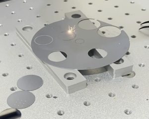
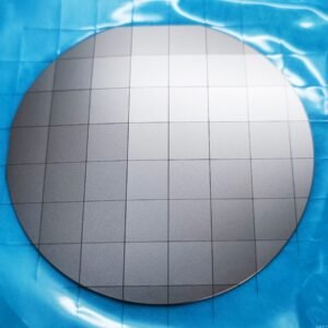
Polycrystalline Silicon Wafer
Cost-Effective Multi-Crystalline Silicon Substrates for Solar, Research & Semiconductor Applications
Polycrystalline Silicon Wafers are widely used silicon substrates composed of multiple crystal grains. Compared with monocrystalline silicon, they offer a more cost-efficient solution for photovoltaic production, materials research, and educational semiconductor applications where large-scale usage and process realism are more important than perfect single-crystal performance.
From solar cell development to university laboratory experiments, polycrystalline silicon remains one of the most widely adopted silicon materials in industrial and academic environments.
- Custom geometry & 1-pc MOQ: Round, square, or rectangular wafers from 1x1 mm to 310x310 mm (thickness 100 μm to 50 mm) precision-machined to your exact blueprints.
- Custom resistivity tuning: Available from ultra-low to ultra-high ranges (< 0.001 to > 10,000 Ω·cm) to eliminate electrical testing variables.
- Ultra-thin wafer processing: High-precision slicing down to ≤ 100 μm with tight TTV control to prevent edge chipping, bow, and warp during post-processing.
- Global supply experience: Top universities, research labs, and leading fabs worldwide trust our monocrystalline silicon wafers for low-volume prototyping.
- Surface Perfection: < 0.5 nm RMS roughness achieved via industry-standard CMP polishing.
Why Polycrystalline Silicon Wafer Matters?
Polycrystalline silicon is not simply a “lower-cost alternative” to monocrystalline silicon. It is a deliberately engineered material system optimized for real-world photovoltaic and research conditions.
It is widely used in:
- Large-area solar energy conversion systems
- Photovoltaic efficiency comparison studies
- Grain boundary physics and defect research
- Cost-sensitive semiconductor prototyping
- Academic teaching and laboratory demonstrations
In many solar research programs, polycrystalline silicon is preferred because it better reflects industrial-scale solar cell behavior.
Grain Boundaries: The Key Structural Difference
Polycrystalline silicon consists of multiple silicon crystals separated by grain boundaries.
These boundaries directly influence material behavior:
- Reduced carrier mobility
- Increased electron-hole recombination
- Higher defect density variation
- Lower theoretical efficiency ceiling compared to monocrystalline silicon
However, these characteristics are not disadvantages in research contexts.
Instead, they make polycrystalline silicon ideal for:
✔ studying recombination mechanisms
✔ analyzing defect distribution
✔ simulating industrial solar cell conditions
✔ evaluating process optimization strategies
Applications of Polycrystalline Silicon Wafer
Photovoltaic (Solar Cell Industry)
Polycrystalline silicon wafers are widely used in photovoltaic manufacturing processes, especially in cost-sensitive solar cell production and performance optimization studies.
They are typically used for:
- solar cell fabrication
- efficiency benchmarking
- process development and testing
University & Research Laboratories
Polycrystalline silicon is a standard material in semiconductor and materials science education.
Common applications include:
- photovoltaic experiment teaching
- grain boundary analysis
- semiconductor material courses
- low-cost fabrication training
👉 Universities prefer poly wafers because they allow higher experiment volume within limited research budgets.
Semiconductor & Prototype Development
While not used for high-end IC fabrication, polycrystalline silicon wafers are widely used in:
- process testing
- low-cost device prototyping
- non-critical semiconductor structures
- experimental fabrication workflows
Technical Specifications
| Parameter | Standard Options | Customization Available |
|---|---|---|
| Growth Method | CZ (Czochralski) / FZ (Float Zone) | Ultra-pure FZ for High Resistivity |
| Diameter | 1" (25.4mm), 2" (50.8mm), 3" (76.2mm), 4" (100mm), 6" (150mm), 8" (200mm), 12" (300mm) | 1×1mm – 310×310mm custom shapes & dies |
| Crystal Orientation | <100>, <111>, <110> | ±0.5° tolerance, custom off-cut & high-index angles |
| Doping Type | P-type (Boron), N-type (Phosphorus, Arsenic, Antimony), Undoped (Intrinsic) | Custom dopant concentration & gradient profiles |
| Resistivity | 0.001 Ω·cm – 10,000 Ω·cm | Ultra-high resistivity (>20,000 Ω·cm) for detector & RF use |
| Thickness | 50µm – 775µm (standard per diameter) | Up to 50mm thick custom substrates |
| Surface Finish | Single Side Polished (SSP), Double Side Polished (DSP), As-cut | Epi-ready, etched, textured surfaces |
| Coatings (Optional) | Thermal SiO₂, Si₃N₄ | Custom thickness, AR/HR coatings for optics |
| Edge Treatment | Rounded, beveled/chamfered | Custom flat/notch per SEMI standard |
| Surface Roughness (Ra) | < 5 Å (Prime), < 3 Å (Epi-ready) | < 0.5 nm RMS ultra-smooth optical grade |
| Surface Condition | As-cut / lapped / polished / textured | / |
| Application | Solar PV, research, education, prototyping | / |
Available Quality Grades
- Research Grade: Cost-effective for academic experiments, proof-of-concept prototyping and educational labs
- Prime Grade: SEMI standard, low defect density, suitable for device fabrication and pilot production
- Epi-Ready Grade: Ultra-smooth, low particle count, optimized for epitaxial growth processes
- Detector / High-Resistivity Grade: FZ-grown, ultra-low impurity, ideal for radiation detectors and high-voltage devices
Polycrystalline vs Monocrystalline Silicon
| Feature | Polycrystalline Silicon | Monocrystalline Silicon |
|---|---|---|
| Crystal Structure | Multiple grains | Single crystal |
| Cost | Lower | Higher |
| Efficiency | Lower | Higher |
| Main Use | Solar industry, research | Semiconductor devices, high-performance electronics |
| Research Value | Grain boundary studies | Ideal lattice behavior |
👉 Simple conclusion:
Monocrystalline = performance-driven
Polycrystalline = cost & scalability-driven
Unlike large wafer manufacturers that focus on high-volume production, we specialize in supporting low-volume research, custom prototyping and small-batch pilot runs for the global scientific community.
1. True No Minimum Order Policy
Order a single 1″ wafer for preliminary testing, or a full cassette for pilot production — no MOQ restrictions, no forced bulk purchases. We serve individual research groups, student projects and large labs equally.
2. End-to-End Customization Capability
From non-standard geometries and custom resistivity tuning to specialized coatings and precision dicing, we can fabricate substrates to match your exact experimental requirements. Send us your blueprint or spec sheet for a tailored solution.
3. Full Traceability & Compliance
Every shipment includes a batch-specific Certificate of Analysis (CoA) with verified data on resistivity, thickness, flatness, defect density and impurity levels. All materials are fully traceable, supporting academic publication requirements and institutional quality control protocols.
4. Fast & Secure Global Delivery
We ship worldwide via DHL, FedEx and UPS, with typical delivery times of 3–7 business days to North America, Europe and Asia Pacific. All wafers are packed in cleanroom-grade cassettes and ESD-safe packaging to prevent contamination and damage in transit.
5. Technical Support From Material Engineers
Our in-house team of semiconductor material specialists provides free pre-sales consultation to help you select the optimal wafer grade, orientation and parameters for your specific application. We also offer post-sales technical support for process troubleshooting.
Faqs:
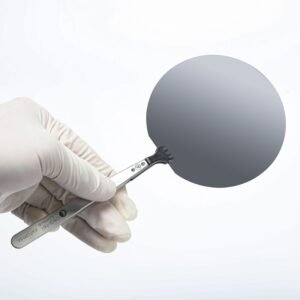
Monocrystalline Silicon Wafer is a single-crystal substrate widely used in university research, semiconductor R&D, and MEMS prototyping. Its uniform crystal structure ensures stable electrical and mechanical properties, making it ideal for experiments requiring high precision and repeatability.
We supply Monocrystalline Silicon Wafers in standard sizes such as 2 inch, 3 inch, 4 inch, 6 inch, 8 inch, and 12 inch. Custom diameter and square wafers are also available for research and special applications.
The price depends on diameter, doping type, orientation, resistivity, and surface polishing (DSP/SSP). Small research quantities are available, and we provide competitive pricing for bulk and OEM orders.
Yes. We supply both P-type (Boron doped) and N-type (Phosphorus or Arsenic doped) Monocrystalline Silicon Wafers. Doping concentration can be customized based on device requirements.
We provide <100>, <111>, and <110> orientations. <100> is most commonly used for IC manufacturing, while other orientations are used for MEMS and research applications.
We offer a wide resistivity range from low resistivity wafers (0.01 Ω·cm) for power devices to high resistivity (>100,000 Ω·cm) wafers for RF, MEMS, and photonics applications.
Yes. We support low MOQ and research orders. Universities and R&D labs can purchase even small quantities for prototyping and testing.
DSP (Double Side Polished) wafers offer higher flatness and better uniformity, while SSP (Single Side Polished) wafers are more cost-effective and commonly used for general applications.
Standard Monocrystalline Silicon Wafers usually ship within 2–4 working days. Custom specifications may require additional processing time depending on requirements.
Yes. We can provide inspection reports including thickness, resistivity, TTV, warp, and surface quality upon request.
Yes. We fully support university labs, research groups, and R&D centers with low MOQ orders. Even single-wafer purchases or small batch orders are available for prototyping, testing, and grant-funded projects.
Yes. We can provide detailed datasheets including resistivity, crystal orientation, doping type, thickness tolerance, TTV, surface roughness, and polishing type. Additional metrology reports can also be supplied for publication or lab documentation purposes.
Most academic labs use 2-inch, 3-inch, 4-inch, and 6-inch Monocrystalline Silicon Wafers for research and teaching purposes. Custom sizes can also be fabricated for specific experimental setups or equipment compatibility.
Yes. We can work with Purchase Orders (PO), institutional billing, and grant-funded procurement systems. Proforma invoices (PI) and quotation documents can be provided for funding applications and internal approval processes.
It depends on the experiment. DSP wafers are preferred for high-precision optical, MEMS, and lithography research due to better flatness and surface quality. SSP wafers are commonly used for general experiments and cost-sensitive academic projects.
Yes. We ship globally, including to universities and research institutions in the United States. Wafers are packed in cleanroom-grade wafer carriers to ensure safe transportation and contamination control.
Yes. Monocrystalline Silicon is one of the most widely used substrates for MEMS devices, photonic structures, sensors, and microfabrication research due to its excellent mechanical stability and well-understood material properties.
REQUEST A QUOTE
Our professional team will reply to you within one business day. Please feel free to contact us!
