
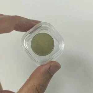
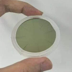
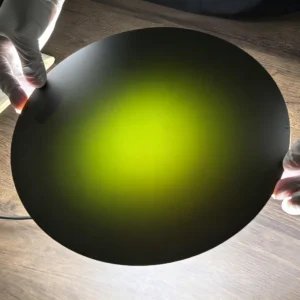
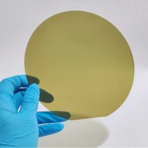
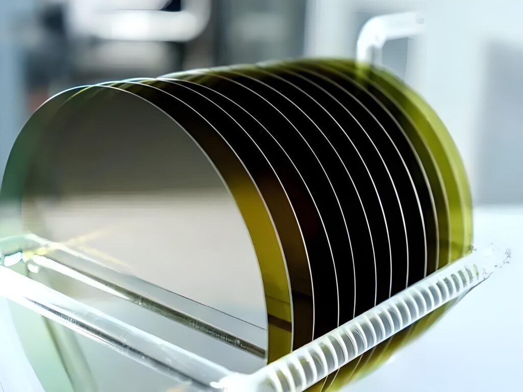
Silicon Carbide (SiC) Substrate
Silicon Carbide (SiC) substrates enable next-generation power efficiency, high-temperature reliability, and superior RF performance. Supwafer supplies epi-ready 4H and 6H SiC wafers with industry-grade metrology, micropipe control, and flexible sizing for R&D and production.
Silicon Carbide (SiC) is a wide-bandgap (WBG) semiconductor that outperforms silicon for high-voltage, high-frequency, and high-temperature applications. Key material advantages:
- Wide bandgap (4H-SiC ≈ 3.26 eV) — enables lower on-resistance and higher breakdown voltages.
- High thermal conductivity (~390–490 W/m·K) — improves heat dissipation in power modules.
- High critical electric field (2–4 MV/cm) — allows thinner drift regions and smaller device footprints.
- Mechanical stability & chemical resistance — robust for harsh environments and long service life.
SiC Polytypes & Conductivity
Common Polytypes
4H-SiC — industry standard for power electronics and RF; best balance of mobility and stability.
6H-SiC — used in some high-temperature sensors and UV LEDs; cost-effective for niche uses.
3C-SiC (cubic) — higher mobility but limited large-scale production; mostly research.
Emerging: 8-inch/8H research and pilot lines are under development; adoption expected to grow.
Conductivity Options
Conductive (n-type) — nitrogen doping for power MOSFETs, diodes.
Semi-insulating (SI) — vanadium compensated or intrinsic; resistivity >10⁹ Ω·cm for RF/microwave substrates and low-loss microwave circuits.
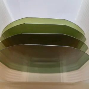
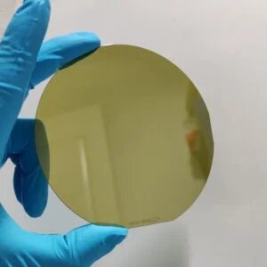
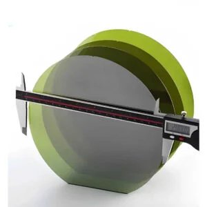


Typical Specifications (Standard & Custom Options)
Supwafer offers standard wafers and custom sizes; tighter tolerances available on request.
| Parameter | Typical Range / Option |
|---|---|
| Diameter/Size | 25 mm(2"), 50mm(4"), 100 mm (4″), 150 mm (6″), 200 mm (8″), 300mm(12"),Square — custom on request |
| Thickness | 350–1,000 µm depending on diameter; custom thickness available |
| Surface finish | Epi-ready CMP, double-side polished (DSP), single-side polished (SSP) |
| TTV (Total Thickness Variation) | ≤5 µm typical (tight control for epi processes) |
| Bow / Warp | ≤40 µm (6″ typical) — tighter specs achievable |
| Micropipe density | <0.1 cm⁻² industrial target; premium grades <0.01 cm⁻² |
| Surface roughness (Ra) | Customize |
| Dislocation density | <10⁴ cm⁻² (target for high-voltage device yield) |
| Epi-ready | Yes — hydrogen anneal & CMP available for epi growth compatibility |
Square Silicon Carbide Substrate
| Size (mm) | Type | Size(mm) | Type |
|---|---|---|---|
| 3x3x0.35 | 4H - N | 5x5x0.35 | 4H - N |
| 8x8x0.35 | 4H - N | 10x10x0.35 | 4H - N |
| 5x10x0.35 | 4H/6H - N | 10x20x0.35 | 4H/6H - N |

- Power electronic devices: Used in manufacturing square-packaged SiC power diodes and MOSFETs (Metal-Oxide-Semiconductor Field-Effect Transistors). They are compatible with scenarios requiring “miniaturization and high integration” such as new energy vehicle electronic control systems and industrial frequency converters, reducing the fitting gap between the substrate and the package housing.
- RF and microwave devices: In high-frequency RF devices for some military radars and satellite communications, square substrates can better match planar circuit designs and reduce signal transmission losses.
- Sensors and special devices: For example, high-temperature pressure sensors and ultraviolet detectors. The square structure facilitates precise alignment with the sensor’s electrodes and package bases; meanwhile, the high and low temperature resistance of silicon carbide ensures the sensors operate stably in extreme environments.
How SiC Substrates Are Manufactured (Key Notes)
Silicon carbide boules are typically grown by Physical Vapor Transport (PVT):
Powder synthesis — high-purity SiC feedstock produced.
Seed mounting — 4H seed attached in growth ampoule.
High-temperature growth — sublimation @ 2300–2500°C deposits SiC on seed forming a boule.
Slicing — diamond wire saw slices wafers from boule.
Polish & inspection — CMP or diamond polishing to epi-ready surface, then metrology & CoA.
Notes & alternatives:
PVT is currently the dominant commercial method for 4H/6H production.
SSM (sublimation sandwich method) and other innovations improve yield and boule size; 8″ efforts are ongoing.
Epi-ready wafers require careful CMP and H₂ anneal to achieve oxide-free surfaces for epitaxy.
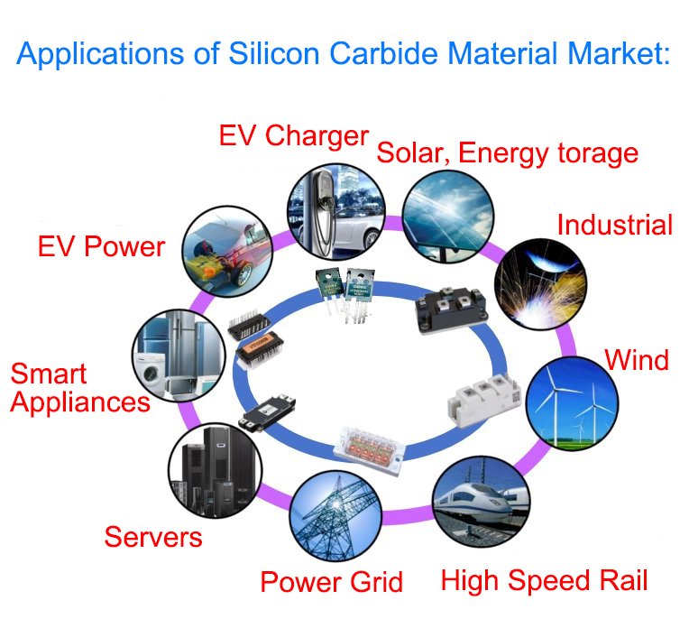
Key Applications & Use Cases
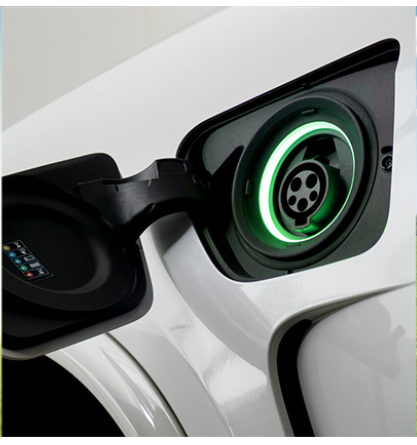
Electric Vehicles (EVs) — SiC MOSFETs and diodes in inverters and onboard chargers reduce switching losses and improve range.
Renewable Energy — solar and wind inverters benefit from higher efficiency and higher operating voltages.
5G & RF — semi-insulating SiC substrates for high-power RF amplifiers and low-loss microwave circuits.
Aerospace & Defense — extreme temperature and radiation tolerance for radar and satellite systems.
Data Centers & Power Supplies — higher efficiency power conversion reduces losses and cooling needs.


Selection Guide — 4 Steps to Choose SiC Substrate
Choose the polytype — 4H for power/RF; 6H for select high-temp applications.
Select conductivity — conductive (n-type) for power devices; SI for RF/microwave.
Match wafer size & epi readiness — 4″ for R&D, 6″ for production, 8″ for upcoming volume scaling.
Verify metrology & CoA — request micropipe density, TTV, resistivity (for conductive types), four-point probe maps, and dislocation counts.
Faqs:
1. What is a SiC substrate, and why is it important in semiconductor applications?
A SiC (Silicon Carbide) substrate is a single – crystal wafer made of silicon carbide. It’s crucial in semiconductors because of its wide bandgap, high thermal conductivity, and high breakdown electric field. These properties enable the development of high – power, high – frequency, and high – temperature electronic devices, outperforming traditional silicon in many harsh – environment and high – performance applications.
2. What are the main crystal structures of SiC substrates, and how do they differ?
3. What methods are used to grow SiC substrates, and what are their advantages and disadvantages?
The main growth method is the physical vapor transport (PVT) method. Advantages include the ability to grow large – diameter (currently up to 6 – inch and beyond) and high – quality single crystals. Disadvantages are high growth temperatures (around 2000–2500 °C), slow growth rates, and the need for precise control of temperature gradients and gas flow. Other methods like chemical vapor deposition (CVD) are used for epitaxial layers but not yet as mature for bulk substrate growth.
4. Can SiC substrates be used with other semiconductor materials in heterostructures?
Yes. For example, GaN (Gallium Nitride) can be epitaxially grown on SiC substrates. The lattice mismatch between SiC and GaN is relatively small, allowing for the fabrication of heterostructure devices. This combination leverages SiC’s high thermal conductivity and GaN’s high electron mobility for high – power and high – frequency applications like RF amplifiers.
5. How does the cost of SiC substrates compare to silicon substrates, and what factors contribute to the difference?
SiC substrates are significantly more expensive than silicon substrates. Factors include the high cost of raw materials, the complex and slow growth process (PVT requires high temperatures and specialized equipment), and lower yields during crystal growth and wafer processing. However, as technology matures and production scales up, costs are gradually decreasing.
6. What are the typical thickness and diameter specifications of commercially available SiC substrates?
Commercially, SiC substrates are available in diameters ranging from 2 inches to 6 inches (and development is ongoing for larger sizes). Thicknesses can vary, but for typical device fabrication, wafer thicknesses are in the range of several hundred micrometers. The thickness is related to mechanical stability during processing and device operation, especially for high – power applications where heat dissipation is critical.
7. What role do SiC substrates play in the development of electric vehicles (EVs)?
In EVs, SiC substrates are used to fabricate power devices (such as MOSFETs and diodes) in the traction inverter. These devices can operate at higher temperatures and voltages, enabling more efficient power conversion, reduced energy loss, and smaller, lighter inverter systems. This contributes to increased driving range and improved overall performance of electric vehicles.
8. How are SiC substrates characterized for quality control during production?
9. How to get SiC substrates with specific crystal orientations?
Source from suppliers or grow in-house by aligning seed crystals with precision fixtures; verify via X-ray diffraction.
10. How to precisely control SiC substrate thickness?
Use in-situ optical interference monitoring, regulate source material via mass-flow controllers, or fine-tune with post-growth thinning.
11. How to overcome SiC brittleness for flexible electronics?
Fabricate ultra-thin layers, combine with flexible polymers via CVD, or use nano/micro-structuring to relieve stress.
12. How to reduce SiC substrate costs for large research projects?
Use recycled/lower-grade substrates (with treatment), optimize growth yield, or collaborate to share costs.
13. What tools simulate SiC growth for optimization?
Use MD for atomic processes, FEA for thermal/mechanical modeling, CFD for gas flow, or specialized semiconductor growth software.
