
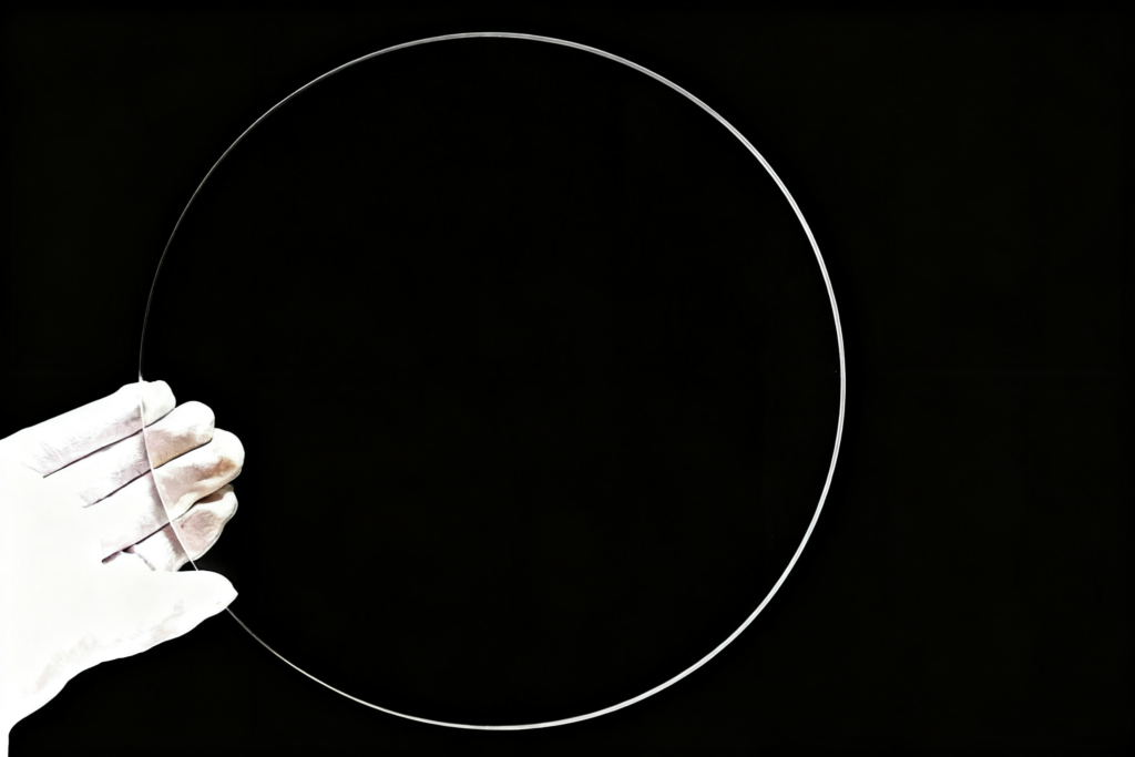
Fused Silica Wafers
Optical Grade JGS1/JGS2 – Supwafer
- High Purity, Contamination-Free Material
- Reliable Substrate for High-Temperature Processes
- Custom Sizes and Surface Finishes Available
Table of Contents
1. What Is a Fused Silica Wafer?
Fused silica wafers are thin, flat discs manufactured by melting ultrapure SiO₂ (≥99.995% purity) and polishing to precise tolerances. Two common production methods define their quality:
- Synthetic Fused Silica: Made from silicon-rich precursors (e.g., SiCl₄) oxidized in a H₂+O₂ atmosphere. Ultra-low impurities (<50 ppm) and controlled OH content make it ideal for optics and semiconductors.
- Fused Quartz: Derived from natural quartz crystals. Slightly higher impurities (~500 ppm) but superior UV transmission—suited for high-temperature lab equipment and UV lithography.
Key Distinction: The terms “fused silica” and “fused quartz” are often used interchangeably, but synthetic fused silica offers higher purity, while fused quartz excels in UV performance.
2. Core Properties (Why Choose Fused Silica?)
Fused silica wafers outperform other glass substrates due to these critical characteristics:
| Property | Specification | Benefit |
|---|---|---|
| Thermal Stability | Low coefficient of thermal expansion (CTE: ~5.8×10⁻⁷/K) | Resists thermal shock;maintains shape at temperatures up to 1200°C |
| Optical Transmission | 90%+ in visible/IR spectra; down to 150 nm (UV) | Ideal for photonic devices, UV lithography, and laser systems |
| Chemical Inertness | Resists acids, solvents, and corrosion | Safe for harsh semiconductor processes (e.g., CVD, etching) |
| Purity | SiO₂ content ≥99.995%; impurities <50 ppm (synthetic) | Prevents contamination in microelectronics and medical devices |
| Mechanical Strength | Surface hardness ~570 KHN; low bow/warp (<40 µm) | Durable for handling, bonding, and thin-film coatings |
3. Common Types & Grades
Fused silica wafers are categorized by grades, each optimized for specific applications. The JGS series (widely used in global markets) is defined below:
| Grade | OH Content | UV Transmission | Best For |
|---|---|---|---|
| JGS1 (UV Grade) | ~1000 ppm | 90% (220–150 nm); drops at >1.2 µm (IR) | UV photolithography, precision optics, and laser systems |
| JGS2 (Optical Grade) | <300 ppm | Starts absorbing <270 nm; 90% up to 2 µm (IR) | MEMS, microfluidics, and general optical substrates |
| JGS3 (Full Spectrum) | <10 ppm | >80% (200 nm–3 µm); 90% (250–2.5 µm) | Advanced photonics, aerospace sensors, and IR imaging |
Other Grades: Corning HPFS (high-purity fused silica) and Dynasil 1000/4000—equivalent to JGS2 for industrial use.
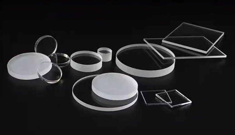
4. Standard Specifications & Sizes
Fused silica wafers are available in round and rectangular formats, with tight tolerances for semiconductor and optical applications.
Supwafer offers a full range of fused silica wafers to meet research and production needs:
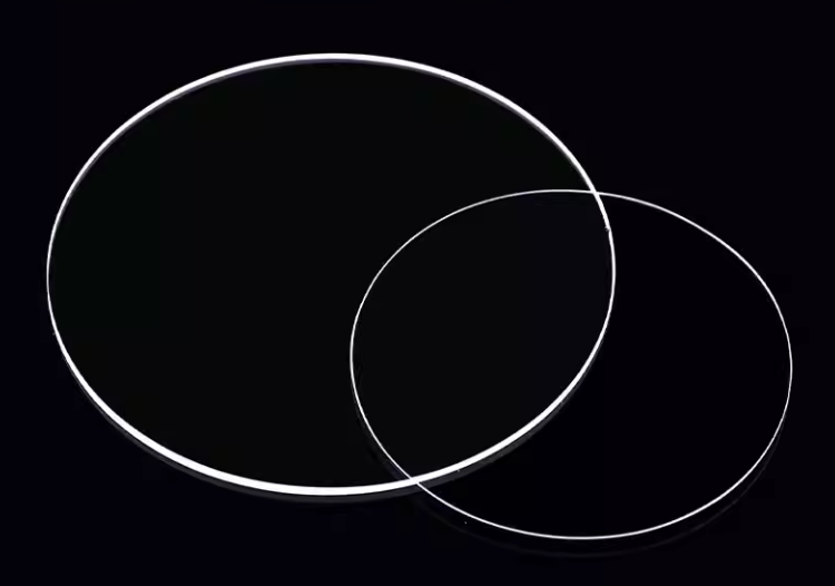
4.1 Round Wafers (Most Common)
| Diameter | Thickness Range | Key Tolerances | Application |
|---|---|---|---|
| 1 inch (25 mm) | 170–1000 µm | TTV <10 µm; no flat | R&D, small sensors |
| 2 inches (50.8 mm) | 200–1000 µm | TTV <10 µm; 1 SEMI flat | MEMS, lab-on-a-chip devices |
| 4 inches (100 mm) | 500–1000 µm | TTV <10 µm; primary flat 32.5 mm | Semiconductor carriers, photomasks |
| 6 inches (150 mm) | 700–1000 µm | TTV <10 µm; 1 flat | Optoelectronics, waveguide circuits |
| 8 inches (200 mm) | 700–1000 µm | TTV <10 µm; SEMI notch | Advanced semiconductor processing |
4.2 Rectangular/Square Wafers
- Sizes: 10×10 mm, 10×20 mm, 25×25 mm, 100×100 mm
- Thickness: 170–1000 µm
- Use Cases: Custom microfluidic chips, sensor arrays, and small-scale optics.
4.3 Surface Finish
- Double-Side Polished (DSP): Standard for most applications; surface roughness Ra <1 nm (critical for thin-film adhesion).
- Single-Side Polished (SSP): Cost-effective for non-optical uses (e.g., dummy wafers).
5. Fused Silica Wafers Key Applications
5.1 Semiconductor Manufacturing
- Photomasks: High optical clarity enables precise patterning in IC production.
- Wafer Carriers/Dummies: Support device wafers during backgrinding; protect equipment from contamination.
- Process Chambers: Resist high temperatures and corrosive gases (e.g., in diffusion furnaces).
5.2 Optics & Photonics
- Lenses, prisms, and filters for lasers, telescopes, and medical imaging.
- Optical fibers: Core material for high-speed data transmission.
5.3 MEMS & Sensors
- Substrates for accelerometers, pressure sensors, and lab-on-a-chip devices (chemical inertness prevents sample contamination).
5.4 Laboratory & Medical
- Beakers, flasks, and tubing: Thermally stable and sterilizable for chemical reactions.
- Medical devices: Miniaturized optical components for diagnostic tools (e.g., DNA sequencers).
6. Why Choose Supwafer?
At Supwafer, we combine expertise, quality, and customization to support semiconductor laboratories, research institutions, and high-tech manufacturers worldwide.
Expertise – Over 10 years of experience supplying wafers to global universities and R&D centers.
Quality Assurance – Each wafer is tested for surface flatness, roughness, and warp to meet ISO and SEMI standards.
Customization – Tailor-made wafer sizes, thicknesses, polishing, and flats/notches.
Trusted by Researchers – Our wafers are used by top research institutions in semiconductor, optics, and materials science.
Global Supply Chain – Reliable logistics and fast shipping worldwide.
Faqs:
1. What is a fused silica wafer and why is it important in semiconductor research?
A fused silica wafer is a high-purity quartz substrate valued for its thermal stability, low expansion, and excellent optical transparency. It is widely used in semiconductor research, MEMS development, photonics, and university laboratory experiments.
2. How does a fused silica wafer differ from standard quartz wafers?
Compared to natural quartz wafers, fused silica wafers offer higher purity, lower thermal expansion, and superior UV transmission, making them a preferred choice for advanced semiconductor and photonics applications.
3. What are the typical thickness options available for fused silica wafers?
Fused silica wafers are available in thicknesses ranging from 200 μm to 2 mm, with customized thicknesses provided for academic research and semiconductor R&D projects.
4. What wafer diameters are standard for fused silica substrates?
Common diameters include 2-inch, 4-inch, 6-inch, and 8-inch fused silica wafers, though custom sizes can be manufactured to meet the needs of university laboratories and industrial users.
5. Can fused silica wafers withstand high-temperature semiconductor processes?
Yes. Fused silica wafers have excellent thermal resistance up to 1000°C, ensuring reliable performance during high-temperature semiconductor fabrication, microfabrication, and optical device testing.
6. Do fused silica wafers provide UV and optical transparency?
Yes. Fused silica wafers feature outstanding UV, visible, and IR transmission, making them ideal for optical research, photonics, lithography, and academic experiments.
7. What are the main applications of fused silica wafers in research and industry?
Fused silica wafers are commonly used for MEMS fabrication, photomasks, semiconductor device prototyping, photonics, and optical sensors. Their high purity and stability make them especially valuable in university R&D labs.
8. Are fused silica wafers suitable for cleanroom semiconductor processing?
Yes. Fused silica wafers are ideal for cleanroom environments because of their high purity, low particle generation, and contamination-free properties, making them widely used in semiconductor manufacturing and university research labs.
9. Can fused silica wafers be used for MEMS fabrication?
Absolutely. Fused silica wafers are a preferred substrate for MEMS fabrication due to their dimensional stability, low thermal expansion, and excellent optical transparency, enabling reliable micro-scale device development.
10. What polishing options are available for fused silica wafers?
Fused silica wafers can be supplied single-side polished (SSP), double-side polished (DSP), or unpolished, depending on research and industrial applications. Polished wafers ensure high surface quality for photonics, optics, and lithography research.
11. How should fused silica wafers be stored in research laboratories?
They should be stored in protective wafer carriers within a clean, dry, and temperature-controlled environment to maintain purity and prevent scratches or contamination — essential for academic and R&D use.
12. Are fused silica wafers resistant to chemicals?
Yes, fused silica offers excellent chemical resistance, making it suitable for semiconductor etching and cleaning processes. The only exception is hydrofluoric acid (HF), which can etch silica substrates.
13. What advantages do fused silica wafers provide in academic research?
For universities and research institutes, fused silica wafers deliver high-precision optical clarity, low expansion rates, and superior stability, making them valuable in nanotechnology, photonics, and semiconductor device research.
14. How are fused silica wafers packaged for international shipping?
To ensure safe delivery, wafers are packed in anti-static wafer carriers with shock-absorbing materials, meeting the requirements of global semiconductor companies and university labs.
15. Where can fused silica wafers be sourced for university laboratories and R&D centers?
High-quality fused silica wafers can be sourced from specialized semiconductor material suppliers that serve both industrial manufacturers and academic research institutions worldwide, ensuring consistent quality and reliable performance.
16. Can fused silica wafers be customized for university research or industrial applications?
Yes. We provide custom fused silica wafers with tailored diameters, thicknesses, surface finishes, and flatness levels, designed to meet the specific requirements of university laboratories, MEMS projects, and semiconductor R&D applications.
17. What customization options are available for fused silica wafers?
Customization includes wafer diameter, thickness, edge profile, surface polishing (single-side or double-side), and optical coatings. These options ensure the wafers meet the unique needs of academic research experiments, photonics development, and high-precision semiconductor processes.
REQUEST A QUOTE
We offer competitive Fused Silica Wafer pricing for laboratories, research institutes, and semiconductor manufacturers worldwide.
