
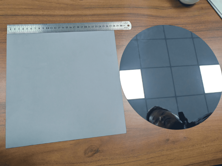
Square Silicon Wafer
High-quality square and rectangular silicon wafers customized for MEMS, semiconductor, and research applications.
Available in various sizes, thicknesses, resistivity ranges, and crystal orientations.
Compared to traditional circular wafers, square wafers enable more efficient die layout during dicing, helping reduce material waste and improve chip utilization.The square geometry also simplifies alignment in packaging processes such as wire bonding and flip-chip assembly, making it suitable for research and prototyping environments.Typical specifications include low total thickness variation (TTV) and consistent electrical performance, supporting reliable device fabrication.
- Custom sizes available
- Fast prototyping & stable supply
- Suitable for R&D and industrial use
Table of Contents
What is a Square Silicon Wafer
A square silicon wafer is a customized silicon substrate shaped into square or rectangular geometry instead of the traditional circular wafer.
Unlike standard wafers used in semiconductor fabs, square wafers are often designed for:
- MEMS fabrication
- Sensors and detectors
- Microfluidics
- Photonics and optics
- Academic research and prototyping
- Semiconductor device development
Their geometry allows better space utilization and easier integration into specific device designs.
Square Silicon Wafer Key Advantages
Higher Material Utilization
Square wafers reduce edge waste compared to circular wafers, improving overall material efficiency.
In practical applications, up to 30% of silicon material can be lost when dicing circular wafers into square dies.
By using square wafers, this loss can be significantly reduced, allowing more usable dies per wafer and lowering material costs.
Simplified Dicing and Packaging
Square geometry reduces unnecessary cutting steps during wafer dicing.
Compared with circular wafers, this can reduce dicing time by up to 50%, especially in prototyping or small-batch production.
During packaging (wire bonding or flip-chip assembly), flat edges improve alignment consistency and handling efficiency.
Improved Alignment Accuracy
Flat edges allow more predictable positioning in automated processes.
This helps reduce alignment errors commonly seen with circular wafers and improves packaging yield and device reliability.
Quality and Manufacturing
Wafers are produced under controlled manufacturing conditions to ensure:
- Stable electrical properties
- Consistent thickness and flatness
- Surface quality suitable for microfabrication
Additional inspection and metrology processes are applied throughout production.
Applications
Square silicon wafers are widely used in:
- Semiconductor device fabrication
- MEMS and sensor development
- Microfluidics and photonics
- Advanced research and prototyping
If you have specific requirements, feel free to send your specifications or drawings.
Custom Square Silicon Wafer
We supply custom square and rectangular silicon wafers designed for research, MEMS, and device fabrication.
- Size Range
From 25 × 25 mm up to 310 × 310 mm
Custom dimensions available based on drawings - Resistivity Range
0.02 Ω·cm to 100,000 Ω·cm
Suitable for both low and high resistivity applications - Material Type
Monocrystalline silicon (standard)
Polycrystalline silicon (available upon request)
- Size Range

Customization Options
- P-type / N-type
- Crystal orientation ⟨100⟩ / ⟨110⟩ / ⟨111⟩
- Thickness and surface finish
- Surface Finish: Single-side polished (SSP)/ Double-side polished(DSP)
- TTV: Low total thickness variation available
- Custom shapes (square, rectangular, irregular)
- Edge finishing (chamfered or sharp edges)
- Ultra-thin wafers
- Oxide / coating options
- Laser cutting or dicing services
Square Silicon Wafer Supplier - Supwafer
FAQS:
1. What are the standard dimensions of commercially available square silicon wafers?
Standard sizes range from 2 inches (50.8 mm) to 12 inches (300 mm), with 4-inch (100 mm), 6-inch (150 mm), and 8-inch (200 mm) being common for research purposes. Custom sizes can also be fabricated upon request.
2. How does the crystallographic orientation of a square silicon wafer affect its electrical properties?
Orientation, such as (100), (110), or (111), impacts carrier mobility and defect density. For example, (100) wafers are preferred for MOSFETs due to lower surface state density, while (111) wafers are suitable for certain optoelectronic applications.
3. Can square silicon wafers be used interchangeably with circular wafers in microfabrication processes?
While most microfabrication techniques (e.g., photolithography, deposition) are adaptable, equipment designed for circular wafers may require custom fixtures or software adjustments for square geometries.
4. What is the maximum thickness of a square silicon wafer that can be reliably processed?
Thicknesses typically range from 100–775 μm for standard wafers. Thicker wafers (up to 1 mm) can be used for mechanical stability, but may increase handling complexity and processing costs.
5. How do I prevent edge chipping during handling of square silicon wafers?
Use vacuum or edge-gripping tools, avoid sudden impacts, and store wafers in anti-static cassettes with proper edge support. Plasma edge passivation can also enhance mechanical durability.
6. What are the key differences in surface roughness requirements between square wafers for semiconductor vs. MEMS applications?
Semiconductor applications demand ultra-smooth surfaces (< 1 nm RMS) to ensure thin-film uniformity, while MEMS devices may tolerate slightly rougher surfaces (1–5 nm RMS) depending on the structure.
7. Can square silicon wafers be annealed at high temperatures without warping?
Warping risk depends on the wafer’s thickness-to-edge ratio, doping concentration, and annealing profile. Using stress-relieving processes (e.g., graded temperature ramping) can mitigate warping.
8. What types of contaminants pose the greatest risk to the performance of square silicon wafers?
Metal ions (e.g., Fe, Cu) and organic residues can introduce defects and alter electrical properties. Particles larger than 0.1 μm may cause yield loss during lithography.
9. How do I select the appropriate doping level for a square silicon wafer in photovoltaic research?
10. Are there any limitations to using square silicon wafers in microfluidic device fabrication?
Sharp corners may cause flow disturbances and bubble entrapment. Rounding the edges or using microchannel designs that avoid corners can mitigate these issues.
11. What inspection techniques are recommended for detecting subsurface defects in square silicon wafers?
12. Can square silicon wafers be bonded to other substrates (e.g., glass, sapphire) without inducing stress?
Anodic bonding and adhesive bonding are common methods. Using intermediate layers with matched thermal expansion coefficients or applying uniform pressure during bonding helps minimize stress.
13. How does the aspect ratio of square silicon wafers impact plasma etching selectivity?
Higher aspect ratios can lead to non-uniform etching due to ion shielding effects. Adjusting gas flow rates, pressure, and bias voltage can optimize selectivity for square geometries.
14. What are the cost implications of using square vs. circular silicon wafers in research?
15. How can I ensure uniform thin-film deposition on square silicon wafers?
16. Are there specific safety considerations when handling square silicon wafers in a laboratory?
17. Can square silicon wafers be reused after failed fabrication attempts?
Reusable wafers can be stripped of deposited layers using wet chemical or plasma etching, but repeated processing may degrade surface quality. Assess the wafer’s integrity via surface profilometry before reuse.
18. How does humidity affect the storage and performance of square silicon wafers?
19. What are the emerging applications of square silicon wafers in advanced research fields?
Current trends include quantum computing (qubit fabrication), flexible electronics (ultra-thin wafers), and 3D integrated circuits (TSV-based stacking).
REQUEST A QUOTE
Our professional team will reply to you within one business day. Please feel free to contact us!
