
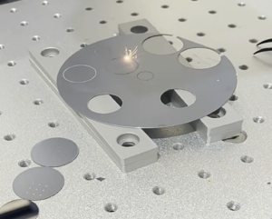
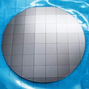
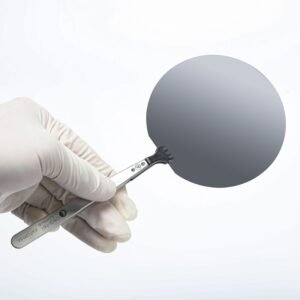
Monocrystalline silicon wafer
High-purity, precision-engineered single crystal silicon substrates tailored for academic labs, research institutes and semiconductor enterprises worldwide. From 1″ research-grade wafers for cleanroom experiments to 12″ prime-grade substrates for pilot production, we deliver SEMI-compliant monocrystalline silicon wafers with tight tolerance control, batch-to-batch consistency and flexible custom configurations. Whether you are fabricating MOSFETs, MEMS sensors, photonic devices or power electronics, our substrates support your innovation with reliable material performance.
- Custom geometry & 1-pc MOQ: Round, square, or rectangular wafers from 1x1 mm to 310x310 mm (thickness 100 μm to 50 mm) precision-machined to your exact blueprints.
- Custom resistivity tuning: Available from ultra-low to ultra-high ranges (< 0.001 to > 10,000 Ω·cm) to eliminate electrical testing variables.
- Ultra-thin wafer processing: High-precision slicing down to ≤ 100 μm with tight TTV control to prevent edge chipping, bow, and warp during post-processing.
- Global supply experience: Top universities, research labs, and leading fabs worldwide trust our monocrystalline silicon wafers for low-volume prototyping.
- Surface Perfection: < 0.5 nm RMS roughness achieved via industry-standard CMP polishing.
Choose Your Solution by Application
Silicon Wafers for Integrated Circuits (ICs) & Discrete Devices
- The Problem: Inconsistent radial dopant profiles and lattice microcracks cause unexpected electrical resistance variations and device drift across your wafer batch, compromising experimental repeatability and prototype performance.
- Our Solution: We provide Prime and Test grade CZ or MCZ wafers with highly uniform radial dopant distribution. Available in heavily or lightly doped variants to perfectly match your solid-state architectures. Ideal for device prototyping and academic research, with no minimum order restrictions.
- Doping Options: N-type (Phosphorus, Antimony, Arsenic) or P-type (Boron, Gallium).
Silicon Wafers for MEMS & Microfabrication Structures
The Problem: Unpredictable etching angles and substrate warping that lead to lithography focus errors and high device failure rates during DRIE (Deep Reactive-Ion Etching).
Our Solution: Substrates engineered with precise crystal orientation control (±0.5° tolerance) and tight Total Thickness Variation (TTV). Our consistent monolithic lattice alignment guarantees highly predictable anisotropic etching results, reducing scrap rates in your microfabrication runs. Available from single prototype wafers to small-batch production.
Orientations: <100>, <110>, <111>, and high-index custom orientations like <211>.
Silicon Wafers for Infrared (IR) Optical Components
The Problem: Subsurface mechanical stress and material impurities causing high absorption and signal loss in the infrared spectrum, degrading detector and optical system performance.
Our Solution: We precision-fabricate optical windows, custom prisms, and reflector substrates from high-purity single-crystal silicon, optimized for outstanding transmission and reflectance performance across near- to far-infrared wavelengths. Ideal for CO₂ laser systems, astronomical optics, and infrared detector arrays.
Value-Added Optics Processing: Custom reflective/anti-reflective coatings designed to your exact specifications.
Silicon Wafers for Next-Gen Photovoltaics (PV) & Green Energy Research
The Problem: Substrate degradation and efficiency loss under high-radiation or prolonged thermal stress, limiting the performance of novel solar cell architectures.
Our Solution: Research-grade P-type and N-type monocrystalline silicon wafers for next-gen PV development. We supply specialized crystal orientations (including <110>) featuring ultra-low oxygen and carbon content to maximize carrier lifetime, as well as flexible ultra-thin substrates optimized for novel flexible cell research and prototyping.
- Available Configurations: Custom thickness, doping, and surface treatments for experimental cell designs.
Silicon Wafers for Power Electronics & High-Voltage Devices
- The Problem: High defect density and low breakdown voltage cause premature device failure and increased conduction losses in IGBT, MOSFET and diode development.
- Our Solution: Low-defect CZ and FZ silicon wafers engineered for power device fabrication, with controlled oxygen content and minimal crystal originated particles (COPs) to enhance gate oxide integrity and breakdown voltage. Custom resistivity ranges support both low-loss conduction and high-voltage blocking requirements.
- Key Specs: Resistivity up to 2,000 Ω·cm, <111> and <100> orientations, low carbon/oxygen impurity levels.
Silicon Wafers for Radiation Detection & High-Energy Physics
- The Problem: Bulk impurities and short minority carrier lifetime reduce charge collection efficiency and energy resolution in particle detectors and radiation imaging systems.
- Our Solution: Ultra-high-purity FZ-grown intrinsic or lightly doped silicon wafers, with extremely low oxygen and carbon contamination and millisecond-level minority carrier lifetime. Optimized for full depletion at moderate operating voltages, delivering consistent response across the entire wafer surface for alpha/beta/gamma and charged particle detection.
- Key Specs: Resistivity 1 kΩ·cm – 20 kΩ·cm, FZ growth, n-type or p-type doping, thickness 200 µm – 500 µm.
Full Specifications & Customization Options
All wafers meet or exceed SEMI M1 standards, with batch-specific Certificate of Analysis (CoA) provided with every order.
Standard Technical Parameters
| Parameter | Standard Options | Customization Available |
|---|---|---|
| Growth Method | CZ (Czochralski) / FZ (Float Zone) | Ultra-pure FZ for High Resistivity |
| Diameter | 1" (25.4mm), 2" (50.8mm), 3" (76.2mm), 4" (100mm), 6" (150mm), 8" (200mm), 12" (300mm) | 1×1mm – 310×310mm custom shapes & dies |
| Crystal Orientation | <100>, <111>, <110> | ±0.5° tolerance, custom off-cut & high-index angles |
| Doping Type | P-type (Boron), N-type (Phosphorus, Arsenic, Antimony), Undoped (Intrinsic) | Custom dopant concentration & gradient profiles |
| Resistivity | 0.001 Ω·cm – 10,000 Ω·cm | Ultra-high resistivity (>20,000 Ω·cm) for detector & RF use |
| Thickness | 100µm – 775µm (standard per diameter) | Up to 50mm thick custom substrates |
| Surface Finish | Single Side Polished (SSP), Double Side Polished (DSP), As-cut | Epi-ready, etched, textured surfaces |
| Coatings (Optional) | Thermal SiO₂, Si₃N₄ | Custom thickness, AR/HR coatings for optics |
| Edge Treatment | Rounded, beveled/chamfered | Custom flat/notch per SEMI standard |
| Surface Roughness (Ra) | < 5 Å (Prime), < 3 Å (Epi-ready) | < 0.5 nm RMS ultra-smooth optical grade |
Available Quality Grades
- Research Grade: Cost-effective for academic experiments, proof-of-concept prototyping and educational labs
- Prime Grade: SEMI standard, low defect density, suitable for device fabrication and pilot production
- Epi-Ready Grade: Ultra-smooth, low particle count, optimized for epitaxial growth processes
- Detector / High-Resistivity Grade: FZ-grown, ultra-low impurity, ideal for radiation detectors and high-voltage devices
Why Partner With Us For Your Research & Prototyping
Unlike large wafer manufacturers that focus on high-volume production, we specialize in supporting low-volume research, custom prototyping and small-batch pilot runs for the global scientific community.
1. True No Minimum Order Policy
Order a single 1″ wafer for preliminary testing, or a full cassette for pilot production — no MOQ restrictions, no forced bulk purchases. We serve individual research groups, student projects and large labs equally.
2. End-to-End Customization Capability
From non-standard geometries and custom resistivity tuning to specialized coatings and precision dicing, we can fabricate substrates to match your exact experimental requirements. Send us your blueprint or spec sheet for a tailored solution.
3. Full Traceability & Compliance
Every shipment includes a batch-specific Certificate of Analysis (CoA) with verified data on resistivity, thickness, flatness, defect density and impurity levels. All materials are fully traceable, supporting academic publication requirements and institutional quality control protocols.
4. Fast & Secure Global Delivery
We ship worldwide via DHL, FedEx and UPS, with typical delivery times of 3–7 business days to North America, Europe and Asia Pacific. All wafers are packed in cleanroom-grade cassettes and ESD-safe packaging to prevent contamination and damage in transit.
5. Technical Support From Material Engineers
Our in-house team of semiconductor material specialists provides free pre-sales consultation to help you select the optimal wafer grade, orientation and parameters for your specific application. We also offer post-sales technical support for process troubleshooting.
Faqs:
Monocrystalline Silicon Wafer is a single-crystal substrate widely used in university research, semiconductor R&D, and MEMS prototyping. Its uniform crystal structure ensures stable electrical and mechanical properties, making it ideal for experiments requiring high precision and repeatability.
We supply Monocrystalline Silicon Wafers in standard sizes such as 2 inch, 3 inch, 4 inch, 6 inch, 8 inch, and 12 inch. Custom diameter and square wafers are also available for research and special applications.
The price depends on diameter, doping type, orientation, resistivity, and surface polishing (DSP/SSP). Small research quantities are available, and we provide competitive pricing for bulk and OEM orders.
Yes. We supply both P-type (Boron doped) and N-type (Phosphorus or Arsenic doped) Monocrystalline Silicon Wafers. Doping concentration can be customized based on device requirements.
We provide <100>, <111>, and <110> orientations. <100> is most commonly used for IC manufacturing, while other orientations are used for MEMS and research applications.
We offer a wide resistivity range from low resistivity wafers (0.01 Ω·cm) for power devices to high resistivity (>100,000 Ω·cm) wafers for RF, MEMS, and photonics applications.
Yes. We support low MOQ and research orders. Universities and R&D labs can purchase even small quantities for prototyping and testing.
DSP (Double Side Polished) wafers offer higher flatness and better uniformity, while SSP (Single Side Polished) wafers are more cost-effective and commonly used for general applications.
Standard Monocrystalline Silicon Wafers usually ship within 2–4 working days. Custom specifications may require additional processing time depending on requirements.
Yes. We can provide inspection reports including thickness, resistivity, TTV, warp, and surface quality upon request.
Yes. We fully support university labs, research groups, and R&D centers with low MOQ orders. Even single-wafer purchases or small batch orders are available for prototyping, testing, and grant-funded projects.
Yes. We can provide detailed datasheets including resistivity, crystal orientation, doping type, thickness tolerance, TTV, surface roughness, and polishing type. Additional metrology reports can also be supplied for publication or lab documentation purposes.
Most academic labs use 2-inch, 3-inch, 4-inch, and 6-inch Monocrystalline Silicon Wafers for research and teaching purposes. Custom sizes can also be fabricated for specific experimental setups or equipment compatibility.
Yes. We can work with Purchase Orders (PO), institutional billing, and grant-funded procurement systems. Proforma invoices (PI) and quotation documents can be provided for funding applications and internal approval processes.
It depends on the experiment. DSP wafers are preferred for high-precision optical, MEMS, and lithography research due to better flatness and surface quality. SSP wafers are commonly used for general experiments and cost-sensitive academic projects.
Yes. We ship globally, including to universities and research institutions in the United States. Wafers are packed in cleanroom-grade wafer carriers to ensure safe transportation and contamination control.
Yes. Monocrystalline Silicon is one of the most widely used substrates for MEMS devices, photonic structures, sensors, and microfabrication research due to its excellent mechanical stability and well-understood material properties.
REQUEST A QUOTE
Our professional team will reply to you within one business day. Please feel free to contact us!
