
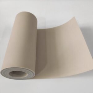
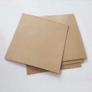
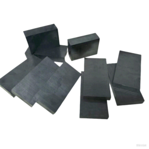
Peek Sheet
Built for harsh conditions, PEEK Sheet delivers exceptional heat resistance, chemical resilience, and strength—ideal for aerospace, semiconductors, and medical fields.We offer customization for any thickness or shape. Choose PEEK Sheet for industry-leading performance that elevates your projects.
- Low outgassing for ultra-clean environments
- Excellent dimensional stability under extreme temperatures
- Superior wear resistance for long-lasting durability
- Electrical insulation to meet strict industry standards
Peek Sheet Manufacturer & Supplier - Supwafer
Wafer Processing Equipment Components
In semiconductor wafer processing, equipment must endure harsh chemical and thermal conditions. For instance, in chemical mechanical planarization (CMP) processes, the traditional materials used in CMP fixed rings often fall short. These processes require components to have high wear resistance, dimensional stability, and chemical resistance. Supwafer’s Peek Sheets step in as a game – changer. Compared to materials like PPS, our Peek – made CMP fixed rings have double the wear resistance. This extended lifespan reduces equipment downtime significantly.
In a high – volume semiconductor manufacturing facility, this can translate to a 3% increase in wafer production capacity. The high – temperature resistance of our Peek Sheets, withstanding up to 260°C, also allows for faster processing as it reduces the need for extended cooling times between processing steps, thus speeding up the overall manufacturing process.


Wafer Handling and Storage
The semiconductor industry demands utmost precision and cleanliness when handling and storing wafers. Any contamination or static discharge can lead to defects in the delicate wafers. Supwafer’s anti – static Peek Sheets are designed for wafer carriers, such as front – opening unified pods (FOUPs) and wafer boxes. The anti – static properties of our Peek Sheets prevent electrostatic discharge, which could otherwise damage the sensitive wafers. Additionally, their low outgassing characteristics are crucial. In a cleanroom environment, even the slightest release of gas or particles can contaminate the wafers.
Our Peek Sheets minimize this risk, ensuring that wafers are stored and transported in a clean, particle – free environment. This significantly reduces the rate of defective wafers, improving the overall yield of the manufacturing process. By providing materials with such tailored properties, Supwafer enables semiconductor manufacturers to enhance the reliability and efficiency of their wafer handling and storage operations
FAQs:
1. What is PEEK sheet?
PEEK sheet is a flat, plate – like form made from polyetheretherketone (PEEK), a high – performance thermoplastic. It combines excellent mechanical properties, high – temperature resistance, chemical resistance, and low – outgassing characteristics, making it suitable for semiconductor applications.
2. What are the main properties of PEEK sheet that make it suitable for semiconductor use?
PEEK sheet offers high – temperature stability, withstanding continuous use at up to 260 °C. It has outstanding chemical resistance to acids, solvents, and cleaning agents used in semiconductor fabrication. Its low – outgassing property is crucial for maintaining a cleanroom environment, and it also provides good electrical insulation and dimensional stability.
3. How does PEEK sheet compare to other materials like POM or PTFE in semiconductor applications?
Compared to POM (polyoxymethylene), PEEK sheet has higher temperature resistance and better chemical resistance. POM is more suitable for non – critical components due to its lower cost, but PEEK outperforms it in harsh semiconductor manufacturing conditions. Against PTFE (polytetrafluoroethylene), PEEK has higher mechanical strength and better wear resistance, while PTFE is more known for its extremely low friction coefficient.
4. What is the thermal conductivity of PEEK sheet, and how does it affect semiconductor processes?
Unfilled PEEK typically has a thermal conductivity around 0.5 W/(m•K). In semiconductor applications, this can be enhanced by adding fillers like carbon fiber or graphite. Good thermal conductivity helps in dissipating heat generated during processes such as wafer handling, reducing the risk of overheating, deformation, and part failure.
5. How well does PEEK sheet resist chemicals used in semiconductor manufacturing, such as etchants and solvents?
PEEK sheet has excellent chemical resistance. It can withstand exposure to strong acids, solvents, and etchants commonly used in semiconductor fabrication processes. This resistance ensures the integrity of components made from PEEK sheet during chemical treatment steps, preventing corrosion and material degradation.
6. What is the electrical insulation property of PEEK sheet, and why is it important in semiconductor applications?
PEEK sheet offers high dielectric strength, making it an excellent electrical insulator. In semiconductor devices, this property is crucial to prevent electrical arcing and short – circuits. It is used in applications like electrical connectors, sockets, and printed circuit board (PCB) supports to ensure the proper functioning of electronic circuits.
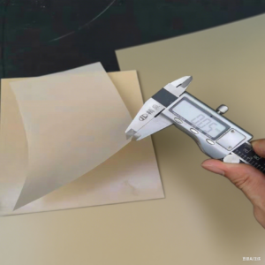
7. How does PEEK sheet perform in terms of dimensional stability during semiconductor manufacturing processes?
PEEK sheet exhibits high dimensional stability, even when exposed to temperature fluctuations and chemical treatments during semiconductor manufacturing. This stability is essential for components such as wafer carriers and fixtures, where precise dimensions are required to ensure accurate processing and alignment of wafers.
8. What is the wear resistance of PEEK sheet, and how does it impact semiconductor equipment?
PEEK sheet has good wear resistance, which is beneficial for components in semiconductor equipment that are subject to repeated mechanical stress, such as wafer handling arms. The low friction and high wear resistance of PEEK help reduce component failure and enhance the longevity of the equipment.
9. Does PEEK sheet have low - outgassing properties, and why are they important in a semiconductor cleanroom?
Yes, PEEK sheet has ultra – low outgassing properties. In a semiconductor cleanroom, outgassing from materials can contaminate the environment and affect the performance of sensitive semiconductor devices. PEEK’s low – outgassing property ensures that it does not introduce unwanted particles or gases, maintaining the cleanliness of the manufacturing environment.
10. How is PEEK sheet used in wafer handling components in semiconductor manufacturing?
PEEK sheet is used to make wafer handling arms, carriers, and fixtures. Its high – temperature resistance, chemical resistance, and dimensional stability make it suitable for these applications. It can withstand the heat and chemicals during wafer processing and ensure accurate positioning and transfer of wafers.
11. Can PEEK sheet be used in chip processing tools, and if so, in what ways?
Yes, PEEK sheet is used in chip processing tools. It can be fabricated into components such as holders, clamps, and guides. Its mechanical strength and chemical resistance allow it to endure the harsh conditions during chip processing, such as exposure to high – temperature and corrosive chemicals.
12. What role does PEEK sheet play in etching equipment in the semiconductor industry?
In etching equipment, PEEK sheet can be used to make parts that come into contact with etchants and wafers. Its excellent chemical resistance to etchants ensures that the equipment components do not corrode during the etching process. Additionally, its dimensional stability helps maintain the accuracy of the etching process.
13. How is PEEK sheet applied in semiconductor chip testing and packaging?
PEEK sheet is used to make test sockets and packaging components. Its dimensional stability ensures precise alignment of chips during testing, and its resistance to harsh chemicals and environmental conditions protects the chips during packaging. The low – outgassing property also helps keep the chip – testing and packaging environment clean.
14. Can PEEK sheet be easily machined into complex shapes for semiconductor applications?
PEEK sheet can be machined using conventional machining techniques such as cutting, drilling, and milling. However, due to its high – temperature resistance and mechanical strength, specialized tools and techniques may be required to achieve high – precision machining. With the right approach, it can be fabricated into complex shapes for semiconductor – specific components.
15. What are the recommended machining parameters for PEEK sheet when making semiconductor components?
When machining PEEK sheet, it is recommended to use high – speed carbide or diamond – coated tools. For cutting, a low feed rate and high cutting speed are often used to prevent overheating and ensure a smooth finish. Drilling may require slow – speed operation with proper cooling to avoid melting the PEEK material. The specific parameters may vary depending on the thickness of the PEEK sheet and the complexity of the shape being machined.
16. How does the cost of PEEK sheet compare to other materials used in semiconductor applications?
PEEK sheet is generally more expensive than common engineering plastics like POM or ABS but may be cost – effective in certain semiconductor applications due to its superior performance. Compared to some high – end materials used in semiconductor manufacturing, such as certain ceramics or specialty metals, the cost of PEEK sheet can be more reasonable while still meeting many performance requirements.
17. Can PEEK sheet be recycled or reused in the semiconductor industry?
PEEK sheet can be recycled to some extent. However, the recycling process for PEEK is more complex compared to some common plastics due to its high – temperature resistance. In the semiconductor industry, where strict cleanliness and quality standards are required, recycled PEEK may be suitable for non – critical applications or components that do not come into direct contact with sensitive semiconductor devices.
REQUEST A QUOTE
Our professional team will reply to you within one business day. Please feel free to contact us!
