
High Resistivity Silicon Wafer (FZ)
100–100k Ω·cm for RF & MEMS | Custom Supplier
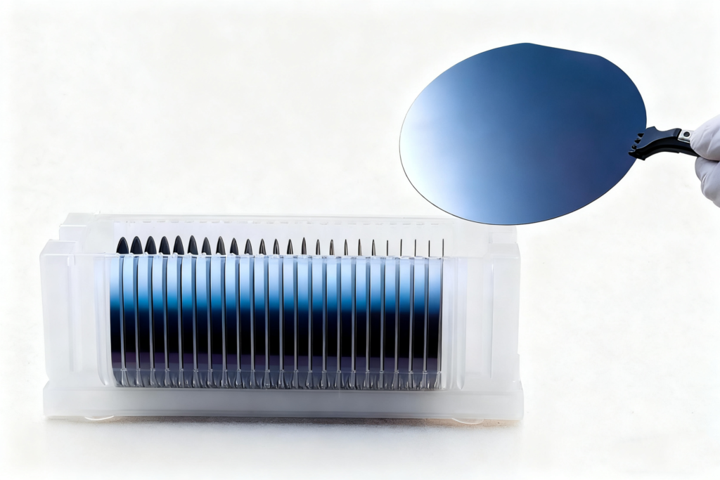
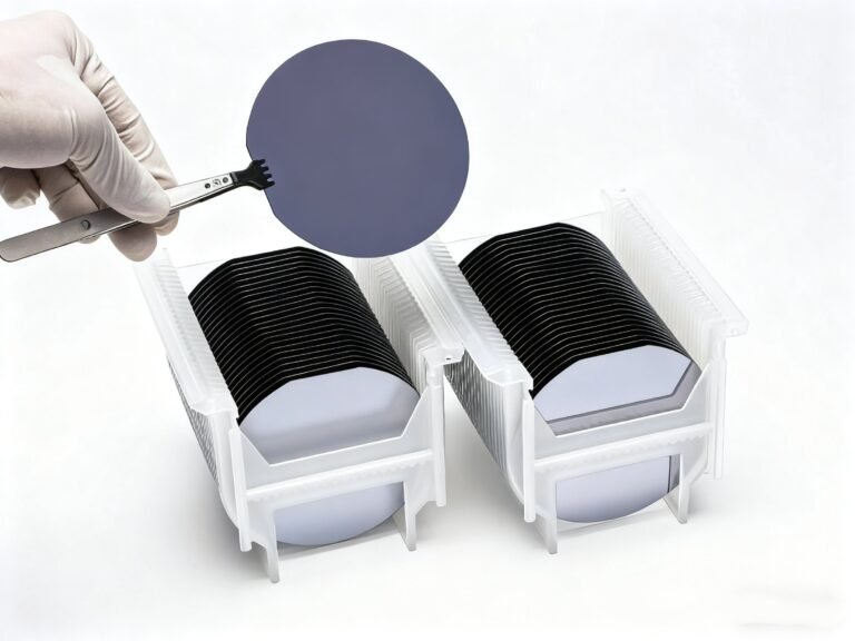
High resistivity silicon wafers (HRSWs) are single-crystal float-zone (FZ) silicon substrates engineered to minimize free carriers and parasitic leakage. With typical resistivity ranges from ≥100 Ω·cm up to 100,000+ Ω·cm, these wafers deliver superior signal integrity for RF/microwave systems, higher breakdown performance for power devices, and ultra-low noise for quantum and sensing applications. Supwafer provides configurable FZ high resistivity silicon wafers, CoA (Certificate of Analysis), and engineering support to help you select the exact wafer grade for your device needs.
- Material: Single-crystal Float Zone (FZ) silicon
- Resistivity: 100 – 100,000+ Ω·cm (typical)
- Common diameters: 100 mm (4") / 150 mm (6") / 200 mm (8") (custom up to 300 mm on request)
- Surface finish: DSP / SSP; Ra typically <1 nm for DSP
- Typical applications: RF/microwave, power electronics, quantum devices, IR sensors, aerospace
Table of Contents
What Is a High Resistivity Silicon Wafer?
High resistivity silicon wafers are engineered substrates with resistivity typically above 1,000 Ω·cm, designed to minimize parasitic conduction and RF signal loss in high-frequency applications.
They are commonly produced using Float Zone (FZ) crystal growth, which avoids oxygen contamination found in standard CZ silicon, enabling ultra-high purity and stable electrical performance. By reducing free carriers (electrons and holes), these wafers significantly lower dielectric loss and substrate interference.
As a result, high resistivity silicon wafers are widely used in RF devices, MEMS sensors, advanced packaging, and other applications requiring high signal integrity and low noise performance.
Why Float Zone (FZ) Matters?
FZ process eliminates contact with a quartz crucible, dramatically reducing oxygen contamination that would limit resistivity.
CZ wafers are common for standard electronics but typically limited to <50 Ω·cm; for true high resistivity (≥100 Ω·cm) applications, FZ is the industry standard.
If your design needs low dielectric loss or ultra-low charge noise, insist on FZ high resistivity wafers and CoA verification.
Technical Specifications (Typical / Available)
Note: Supwafer offers standard specs below; tighter tolerances or custom grades available on request.
| Parameter | Typical Range / Option | Notes |
|---|---|---|
| Resistivity | 100 – 10,000+ Ω·cm | N-type or P-type; ultra-high resistivity tiers on request |
| Wafer diameter | 100 mm, 150 mm, 200 mm (custom up to 300 mm) | Round or square sections available |
| Thickness | 380–775 μm (typical by diameter); custom 100–1500 μm | Thickness tolerance ±5–25 μm depending on spec |
| Surface finish | DSP (double-side polished), SSP (single-side polished) | DSP Ra <1 nm typical |
| TTV (Total thickness variation) | ≤5–10 μm typical | Tight TTV available for high precision needs |
| Warp / Bow | ≤25 μm typical | Controls automated handling & lithography yield |
| Resistivity uniformity | ±5–10% across wafer | Critical for RF and power device uniformity |
| Crystal orientation | <100> (common) / <111> available | <100> preferred for most RF and CMOS process compatibility |
Wafer Types & Grades
By Resistivity Tier:
Standard high resistivity: 100–5,000 Ω·cm — broad use in RF and power sensors.
Ultra-high resistivity: >5,000 Ω·cm — specialized for quantum computing qubits and ultra-low noise sensors.
By Doping:
N-type FZ HRSW — phosphorus/arsenic doped; often used in low-noise RF and space applications.
P-type FZ HRSW — boron doped; preferred in some high-voltage power applications and radiation-tolerant designs.
High Resistivity Silicon Wafer Primary Applications
Our high resistivity silicon wafers are widely used in advanced semiconductor and research applications where low loss, high isolation, and stable electrical performance are critical:
RF & Microwave Devices
- Low dielectric loss and minimal substrate leakage for SAW/BAW filters, RF switches, and high-frequency modules (5G/6G).
Power Electronics
- higher breakdown voltages and lower leakage for IGBTs, Schottky diodes, and EV inverters.
MEMS & Sensors
- Ideal substrates for microfabricated sensors where electrical isolation and substrate control are essential.
Advanced Packaging & Interposers
Used in silicon interposers and heterogeneous integration for high-density signal routing.
Photonics & Optical Integration
Supports low-loss signal transmission in photonic and optoelectronic devices.
Quantum Computing & Research
- Ultra-high resistivity minimizes charge noise and improves device stability in quantum and low-noise environments.
How to Select the High Resistivity Silicon Wafer?
Define Resistivity Target — map device needs to resistivity range (e.g., RF: 500–2,000 Ω·cm; Power: 100–500 Ω·cm; Quantum: >5,000 Ω·cm).
Confirm Growth Method — require Float Zone (FZ) on datasheet/CoA.
Check Uniformity & Tolerances — request TTV, warp/bow, and resistivity uniformity specs.
Verify Material Certification — ask for CoA, four-point probe maps, and supplier test reports (SIMS, FTIR if OH content critical).
Partner with a Reliable Supplier — Choosing a trusted manufacturer is as important as defining technical specs. Supwafer specializes in high-purity Float Zone production and delivers High Resistivity Silicon Wafers with tight uniformity, full CoA documentation, and customizable diameters and orientations. By sourcing directly from Supwafer, you can quickly obtain technical support and competitive pricing while ensuring your wafers meet the exact resistivity target for RF, power or quantum applications.
Customization Options
We support full customization:
- Resistivity range (1k–10k Ω·cm or higher)
- Wafer size & thickness
- Orientation & doping type
- Surface finish (SSP / DSP)
- Special coatings (SiO₂, Si₃N₄, etc.)
Why Choose Us?
Precision Resistivity Control
We ensure stable resistivity across the wafer, reducing variation and improving device consistency.
Clean Surface & Low Defect Density
Strict polishing and inspection processes minimize particles, micro-cracks, and contamination risks.
Flexible Customization
From diameter and thickness to doping and orientation — fully tailored to your project needs.
Fast Response & Engineering Support
Our team supports both R&D and industrial customers with fast quotes and technical guidance.
Faqs:
1. What is High Resistivity Silicon?
High Resistivity Silicon Wafer refers to silicon material with a resistivity typically ≥ 100 Ω·cm and up to several kΩ·cm. It is produced mainly by the Float Zone (FZ) process to achieve extremely low impurity and defect levels. Such wafers are ideal for RF, microwave, detector and sensor applications where low dielectric loss is critical.
2. What is the resistivity range of silicon wafers?
Standard silicon wafers for CMOS or power devices usually range from 0.001 Ω·cm to 10 Ω·cm depending on doping. A High Resistivity Silicon Wafer starts from 100 Ω·cm and can reach several thousand Ω·cm, offering very low free-carrier concentration.
3. What is the difference between 100, 110 and 111 wafers?
These numbers denote crystal orientations. (100) wafers are most common in CMOS fabrication; (111) wafers offer better thermal stability and are often used for MEMS or epitaxial growth; (110) wafers are chosen for high-mobility devices and specific etching properties.
4. What is the resistivity of silicon semiconductors?
Intrinsic silicon at room temperature has about 2.3 kΩ·cm. By doping, the resistivity can be tailored from 0.001 Ω·cm up to several kΩ·cm. High Resistivity Silicon Wafers manufactured by the FZ method provide the upper end of this range.
5. Which semiconductor has the highest resistivity?
Among common semiconductors, semi-insulating SiC or GaAs can reach 10⁷–10⁹ Ω·cm. Within the silicon family, Float-Zone High Resistivity Silicon Wafers (≥10 kΩ·cm) are among the highest.
6. What causes silicon wafers to have high resistivity at the atomic level?
High resistivity arises from extremely low dopant and defect concentrations. The Float-Zone process avoids contact with quartz crucibles and minimizes oxygen, leading to very low free-carrier density and high resistivity.
7. What factors lead to high resistivity?
Low carrier concentration, compensation doping, crystal purity, and wide band gap all contribute. High Resistivity Silicon Wafers combine these factors to achieve stable resistivity and low dielectric loss.
8. What is the unit of wafer resistivity?
The standard unit is ohm-centimeter (Ω·cm), defined by ASTM and SEMI specifications. For thin films, sheet resistance may also be expressed in Ω/sq, but bulk wafer resistivity uses Ω·cm.
9. How quickly can you deliver custom-ordered wafers?
Standard lead time for custom wafers is 4 – 6 weeks. Urgent orders can be expedited within 2 – 3 weeks for an additional fee.
10. Can wafers be pre-cleaned for immediate use in cleanroom environments?
Dopant type and concentration, temperature, defects, crystal orientation, and bandgap determine resistivity. In High Resistivity Silicon Wafers, controlling oxygen and carbon levels is also essential.
11. How do you ensure resistivity stability over long storage periods?
Our wafers are stored in nitrogen-filled chambers to prevent oxidation. Shelf life exceeds 12 months under recommended conditions.
12. What support do you offer for troubleshooting wafer-related issues?
Our technical team provides 24/7 support, including on-site assistance for complex research projects.
13. Are your high-resistivity wafers suitable for cryogenic applications?
Yes, our wafers maintain resistivity stability down to 4K, making them ideal for quantum computing and low-temperature electronics research.
14. Can you provide samples for evaluation before bulk ordering?
We offer sample wafers at reduced cost. Contact us with your project details to request samples.
15. What factors affect the resistivity of semiconductors?
Dopant type and concentration, temperature, defects, crystal orientation, and bandgap determine resistivity. In High Resistivity Silicon Wafers, controlling oxygen and carbon levels is also essential.
16. What general factors influence resistivity?
All materials show resistivity changes with impurity levels, temperature, and structural defects. High purity Float-Zone silicon maintains its specified resistivity more consistently.
17. What is the difference between resistance and resistivity?
Resistance (R) is a property of a specific piece with length and cross-section, while resistivity (ρ) is an intrinsic material property. They are related by R=ρ L/AR = \rho \, L / AR=ρL/A.
18. Does resistivity depend on temperature?
Yes. In metals, resistivity increases with temperature; in semiconductors and insulators, resistivity typically decreases as temperature rises because more carriers are thermally excited. High Resistivity Silicon Wafers exhibit this temperature dependence as well.
19. Why is high resistivity important for RF devices?
High resistivity reduces substrate losses and improves signal integrity, making it ideal for high-frequency circuits.
20. What is the difference between FZ and CZ silicon wafers?
FZ wafers offer higher purity and resistivity, while CZ wafers are more cost-effective and widely used.
REQUEST A QUOTE
Request High Resistivity Silicon Wafer Price
