
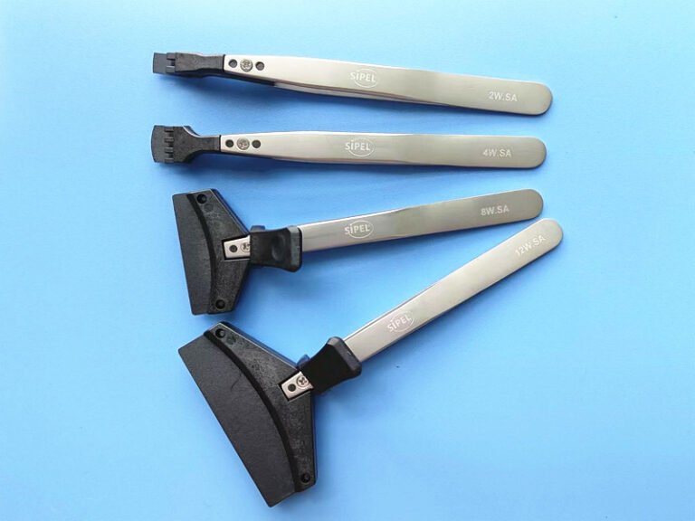
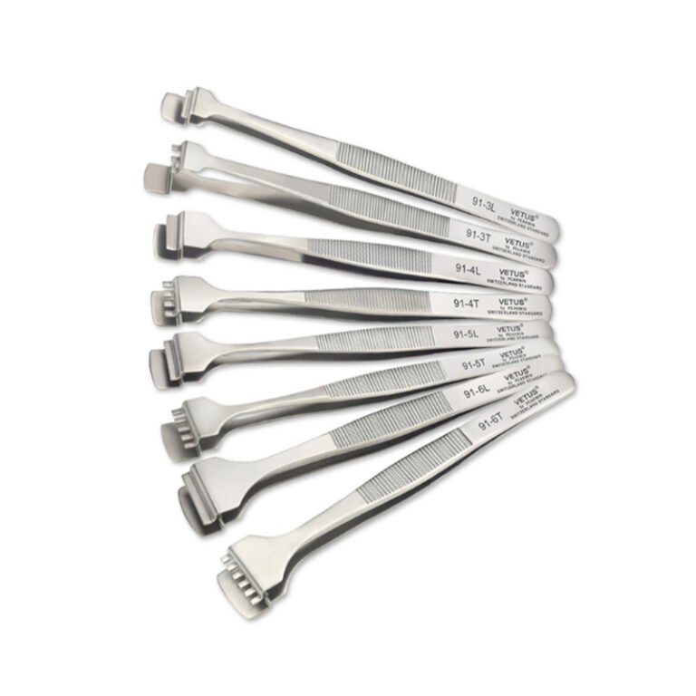
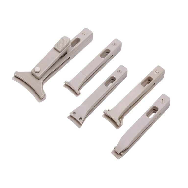
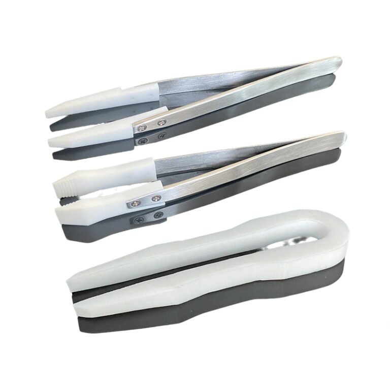
Wafer Tweezers
- Interchangeable tips and adjustable grip adapt to thin - film transistors or composite materials, fitting your unique research needs.
- Made from low-outgassing materials, meeting ISO 14644 standards to prevent particle contamination in precision experiments.
- Aerospace - grade materials resist wear and corrosion, reducing replacement costs and freeing up funds for research
Wafer Tweezers Supplier
Wafer tweezers are specialized tools designed for the delicate handling of wafers, which are thin slices of semiconductor materials like silicon or gallium arsenide, as well as other fragile substrates such as ceramic or glass in laboratory and industrial settings. These tweezers are engineered with precision to meet the stringent requirements of semiconductor and material research.
Key Features:
- Material Composition: They are often made from anti – magnetic materials, such as special stainless – steel alloys or titanium. This property is crucial as it prevents any interference with magnetic fields, which could otherwise affect sensitive semiconductor components. Additionally, materials with high chemical resistance are used to withstand exposure to various acids, solvents, and other harsh chemicals commonly encountered in semiconductor manufacturing and material processing.
- Tip Design: The tips of wafer tweezers come in a variety of shapes. Flat – tipped tweezers provide a broad contact area, reducing the risk of scratching the wafer surface. Pointed – tipped tweezers offer enhanced precision, useful for accessing small or hard – to – reach areas on the wafer. Some tweezers even have angled tips for better maneuverability in confined spaces. The tips may also be coated with materials like Teflon to further minimize friction and prevent scratches.
- ESD Protection: Electro – static discharge (ESD) can severely damage semiconductor wafers. Many wafer tweezers are designed with ESD – safe features, either through the use of conductive materials that dissipate static charges or special coatings that prevent the build – up of static electricity.
Application Areas
- Semiconductor Manufacturing: In the production of integrated circuits, wafer tweezers are used at various stages, from handling wafers during deposition and lithography processes to moving them between different manufacturing equipment.
- Materials Research: In materials science laboratories, these tweezers are used to manipulate and study thin – film materials, composite materials, and other delicate samples. For example, when working with 2D materials like graphene, precise handling with wafer tweezers is crucial to avoid damaging the fragile structure.
- Microelectronics and Photonics: They are also widely used in the assembly and handling of microelectronic components and photonics devices, where high – precision manipulation of small and sensitive parts is required.
Advantages of Our Wafer Tweezers
- Exceptional Precision: Our tweezers are crafted with micron – level accuracy, ensuring that even the most delicate wafers can be handled with the utmost care. The tips are precisely machined to provide a consistent and reliable grip, minimizing the risk of misalignment or damage during handling.
- Customizability: We offer a range of customization options. You can choose from different tip shapes, sizes, and materials to suit your specific application needs. Whether you are working with small – diameter wafers or require a particular tip design for a unique experimental setup, our customizable tweezers can be tailored to your requirements.
- High – Quality Materials: Our wafer tweezers are made from top – grade anti – magnetic and chemically resistant materials. This not only ensures long – lasting performance but also provides excellent protection against environmental factors that could potentially affect the wafers. The materials used are carefully selected to meet the strictest industry standards, guaranteeing reliability and durability.
- ESD – Safe Design: Our tweezers are designed with advanced ESD – protection features. The materials and construction are optimized to effectively dissipate static charges, providing an extra layer of protection for sensitive semiconductor wafers. This helps to prevent ESD – related damage, which can be costly and time – consuming to rectify in research and manufacturing processes.
Faqs:
1. What materials are commonly used for semiconductor wafer handling tweezers?
Common materials include stainless steel for general – purpose use due to its durability and corrosion resistance. Tungsten – carbide – tipped tweezers offer high hardness and wear resistance, ideal for repeated handling of hard wafers. For applications requiring low magnetic interference, non – magnetic alloys like titanium or special stainless – steel blends are preferred. Additionally, ESD – safe polymers can be used to prevent electrostatic damage to sensitive wafers.
2. How do tip designs affect wafer tweezer performance?
- Flat tips: Minimize surface scratches, suitable for general wafer pickup.
- Pointed tips: Enable precision in tight spaces but require careful use to avoid damage.
- Angled tips: Facilitate handling under microscopes or inside probe stations.
3. Why is ESD protection critical for wafer tweezers?
ESD-safe tweezers (with conductive coatings or materials) dissipate static charges, preventing gate oxide breakdown or contamination on wafers during handling.
4. How to select tweezer size for different wafer diameters?
- 50–100mm wafers: Use compact tweezers with short arms for maneuverability.
- 200–300mm wafers: Opt for longer arms and broader tips to ensure stable support.
5. Can wafer tweezers be used for backside handling?
Yes, but choose tweezers with soft-tipped inserts or cushioning to avoid scratching the backside. Some models feature reversible tips for front/back compatibility.
6. How do I maintain the sharpness of tweezer tips?
Avoid using tweezers to handle hard or abrasive materials other than wafers. Regularly clean the tips to remove any debris or residue. If the tips become dull, some high – quality tweezers can be professionally sharpened, but this should be done carefully to avoid damaging the overall structure.
7. What is the role of anti-magnetic properties in wafer tweezers?
In semiconductor applications, especially those involving magnetic – sensitive components or processes, anti – magnetic tweezers prevent interference with magnetic fields. This is important to avoid misaligning magnetic sensors on the wafer or affecting the performance of magnetic – based manufacturing equipment.
8. How do different coating materials on tweezers affect wafer handling?
Coatings such as PTFE (Teflon) reduce friction between the tweezers and the wafer, making it easier to release the wafer without sticking. Diamond – like coatings (DLC) enhance the hardness and wear resistance of the tweezers, prolonging their lifespan. Gold or nickel plating can be used for anti – corrosion and to prevent oxidation, which could contaminate the wafer.
9. Are there cleanroom-specific wafer tweezers?
Yes—cleanroom-rated tweezers use particle-free materials (e.g., PTFE coatings) and undergo pre-cleaning to meet ISO 14644 standards. Regular in-cleanroom maintenance is essential.
10. Why choose anti-magnetic tweezers for semiconductors?
Anti-magnetic alloys (e.g., titanium) prevent interference with magnetic sensors on wafers or equipment like mass spectrometers during processing.
11. How do coatings like PTFE or DLC benefit wafer tweezers?
- PTFE: Reduces friction for smooth wafer release.
- DLC (Diamond-Like Carbon): Enhances wear resistance, extending tweezer lifespan.
- Gold plating: Prevents corrosion and contamination.
12. Can wafer tweezers be customized for unique applications?
Yes—customizations include tip geometry (e.g., serrated edges for grip), built-in heating elements, or force-sensing sensors for R&D projects.
13. What risks arise from using worn tweezers on wafers?
Worn tips may scratch wafers, while loose joints can cause inconsistent grip—increasing the risk of dropping or damaging fragile wafers (e.g., thin SOI substrates).
14. How to store wafer tweezers to prevent damage?
Store in ESD-safe cases or anti-static bags, away from dust and corrosive environments. Use tip protectors to avoid accidental bending or dulling.
15. Are there industry standards for wafer tweezer dimensions?
While not standardized, most tweezers comply with SEMI guidelines for cleanliness and ESD protection. Tip tolerances often range from ±0.01mm for precision models.
16. Why adjust grip force on wafer tweezers?
Adjustable force settings (e.g., spring-loaded mechanisms) allow handling thin wafers without cracking, or securing heavy wafers during transfer.
17. How do wafer tweezers differ from die-handling tweezers?
18. Can wafer tweezers be used in vacuum environments?
REQUEST A QUOTE
Our professional team will reply to you within one business day. Please feel free to contact us!
