
Zinc Oxide (ZnO) Substrate
Zinc Oxide (ZnO) substrate is a single-crystal or polycrystalline thin slice of zinc oxide with exceptional optical, electrical, and piezoelectric properties. As a wide-bandgap semiconductor material, ZnO substrate serves as the foundation for growing various thin films and nanostructures in optoelectronic, piezoelectric, and high-temperature electronic applications .
- 99.99% High Purity,<1.8% GaN Lattice Mismatch, Low Defect Density for Stable Device Performance
- Full Customization (Size/Orientation/Surface), MOQ=1, Fits R&D & Mass Production
- Superior to Sapphire/SiC, 3.73eV Bandgap, Cost-Effective
- Strict QC, 3-8 Week Lead Time, Global Shipping & Professional Technical Support
What is ZnO Substrate (Zinc Oxide Substrate)?
ZnO Substrate (Zinc Oxide Substrate) is a wide-bandgap semiconductor substrate material based on zinc oxide (chemical formula: ZnO). It features a wurtzite hexagonal crystal structure with a bandgap of 3.37-3.73 eV at room temperature and an exciton binding energy as high as 60 meV—far exceeding GaN’s 25 meV. This unique combination enables excellent excitonic luminescent properties at both room and high temperatures. As a critical foundational material in optoelectronic, piezoelectric, and high-temperature electronic devices, zinc oxide substrate has emerged as a promising alternative to traditional substrates, particularly demonstrating significant advantages in GaN thin film epitaxial growth applications.
Key Properties & Advantages of ZnO Substrate:
1. Excellent Optical & Electrical Performance
- Wide Bandgap & High Exciton Binding Energy: The 3.37-3.73 eV bandgap covers the near-ultraviolet (UV) spectrum, and the 60 meV exciton binding energy ensures high-efficiency luminescence, making it an ideal material for UV LEDs and lasers;
- High Transmittance: Transmittance exceeds 50% in the visible to near-UV range (2mm thickness, 400-600nm wavelength), suitable for transparent electronic device requirements;
- Tunable Conductivity: Intrinsically an n-type semiconductor, high conductivity can be achieved through doping with Al, Ga, or In, while bandgap adjustment is possible via Mg doping to meet diverse device needs.
2. Superior Structural & Physical Characteristics
- Lattice Matching Advantage: Sharing the same crystal structure as GaN with extremely low lattice mismatch, using ZnO substrate for GaN thin film epitaxy can increase GaN (002) plane coverage by approximately 45%, significantly optimizing film quality;
- Excellent Mechanical & Thermal Stability: Mohs hardness of 4.0, density of 5.7 g/cm³, and melting point up to 1975℃. Thermal expansion coefficients are 6.5×10⁻⁶/℃ along the a-axis and 3.7×10⁻⁶/℃ along the c-axis, adapting to high-temperature device operating environments;
- High Electromechanical Coupling Coefficient: Exhibits significant piezoelectric effect, suitable for surface acoustic wave (SAW) devices, piezoelectric sensors, and related applications.
3. Environmental Friendliness & Cost Advantages
Abundant and low-cost raw materials (zinc and water); water can be used as an oxygen source to achieve non-toxic, green production. Additionally, some preparation processes (such as hydrothermal method) feature simple equipment and low costs, facilitating large-scale mass production.
Typical Specifications (Standard & Custom Options)
Supwafer offers standard and custom sizes; tighter tolerances available on request.
| Property | Value | Significance |
|---|---|---|
| Crystal Structure | Hexagonal wurtzite | Provides excellent symmetry for epitaxial growth |
| Bandgap | 3.73 eV (room temperature) | Enables UV and visible light applications |
| Exciton Binding Energy | 60 meV | High stability for excitonic devices |
| Transparency | High (visible range) | Ideal for optical devices |
| Piezoelectric Coefficient | Large | Essential for sensors and actuators |
| Refractive Index | 2.0681/2.0510 | Valuable for optical coatings and waveguides |
| Melting Point | 1975°C | High thermal stability for extreme environments |
| Mohs Hardness | ~4.5 | Moderate hardness for handling and processing |
| Purity | 99.99% (typical) | Ensures low defect density and high performance |
ZnO Substrate Supplier - SUPWAFER
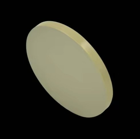
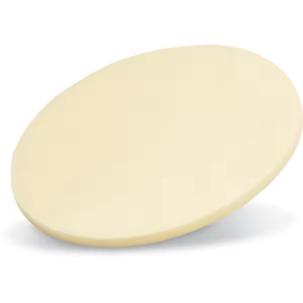
Standard Sizes:
- 5mm × 5mm × 0.5mm
- 10mm × 10mm × 0.5mm
- 20mm × 20mm × 0.5mm
Crystal Orientations:
- c-plane (0001): Most common for epitaxial growth
- a-plane (10-10): For specific optical and electronic properties
- m-plane (10-11): Used in specialized piezoelectric applications
Surface Finishes:
- Single-Side Polished (SSP): Ra ≤ 0.5nm
- Double-Side Polished (DSP): Both surfaces ultra-smooth
Growth Methods:
- Hydrothermal Growth: Produces high-purity single crystals with excellent uniformity
- Vapor Phase Transport: Used for large-diameter crystals
- Molecular Beam Epitaxy (MBE): Enables atomic-level precision for research-grade substrates
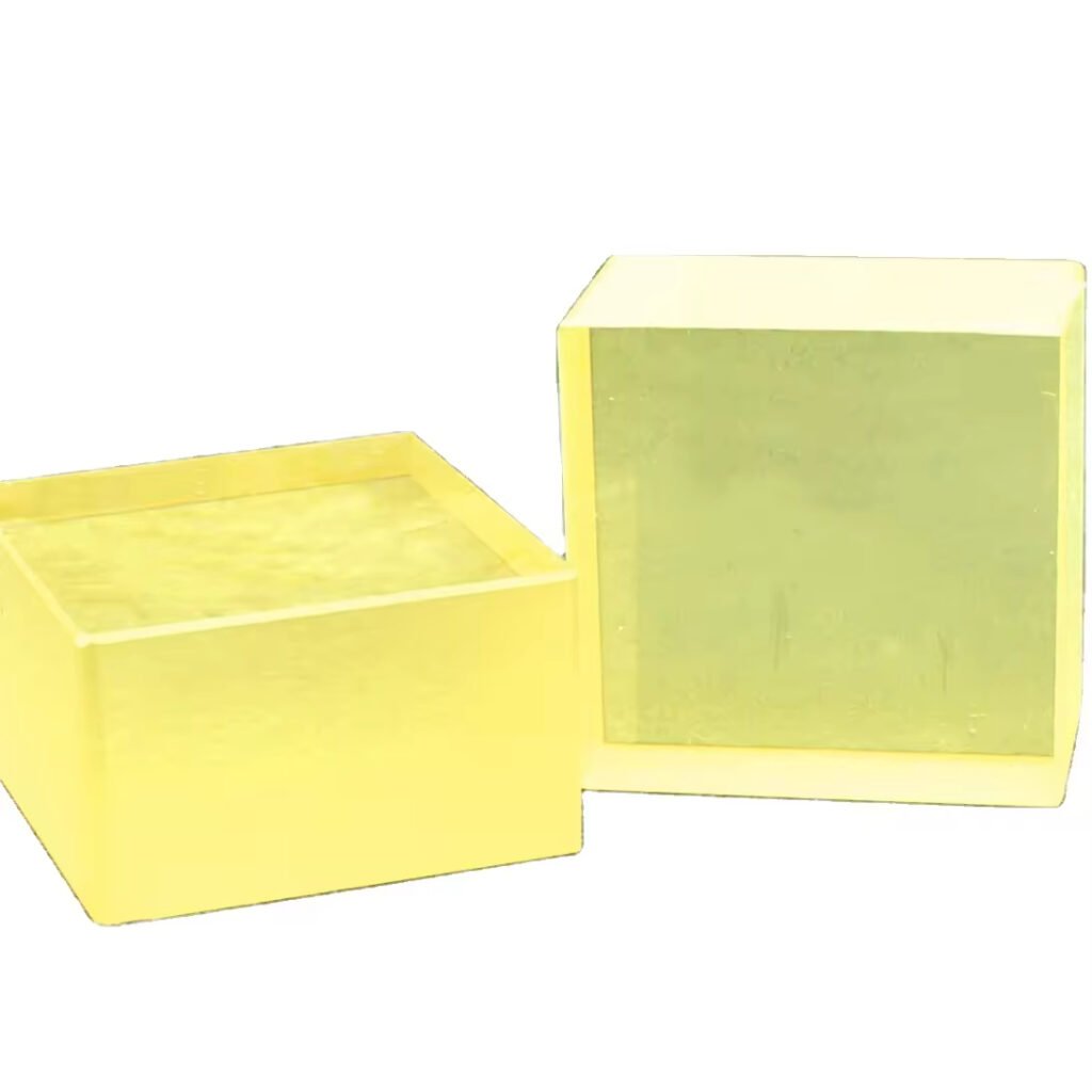
Square ZnO Substrate
We also offer custom services for other sizes. For details, please contact us for support.

Advantages Over Other Substrates
Compared to other substrates, ZnO Substrate has its own unique advantages.
Compared to Sapphire:
- Superior Lattice Match for GaN: 1.8% mismatch vs. 14% for sapphire, resulting in fewer defects
- Higher Transparency in UV Range: Enables more efficient UV device operation
Compared to SiC:
- Lower Cost: More economical for research and niche applications
- Easier Wet Etching: Facilitates simpler device fabrication processes
Compared to Silicon:
- Wider Bandgap: Prevents leakage currents in high-voltage applications
- Natural Piezoelectricity: Eliminates need for additional piezoelectric layers
Key Applications of ZnO Substrate
1. GaN Epitaxy Substrate
- LED Manufacturing: Ideal for growing high-quality GaN films for blue and UV LEDs
- High-Efficiency Devices: The near-perfect lattice match (only 1.8% mismatch) with GaN enables superior crystal quality
- Research & Development: Preferred substrate for GaN-based device research
2. Optoelectronic Devices
- UV Detectors: Excellent responsivity to ultraviolet light
- Photovoltaic Cells: Used as window layers in solar cells
- Transparent Conductive Films: Forms highly transparent and conductive coatings for displays and touch panels
3. Wireless & High-Frequency Applications
- 5G+ Communication Components: Suited for high-frequency devices beyond 5GHz
- Surface Acoustic Wave (SAW) Devices: Utilizes piezoelectric properties for filters and resonators
4. Sensor Technology
- Gas Sensors: Detects harmful gases like H₂S with high sensitivity
- Biomedical Sensors: Biocompatible for medical diagnostic devices
- Pressure & Strain Sensors: Converts mechanical stress into electrical signals
5. Specialized Applications
- High-Temperature Electronics: Operates efficiently in extreme thermal conditions
- Energy Limiter Devices: Handles high peak energy applications
- Piezoelectric Actuators: Used in precision positioning systems
Faqs:
1. What is the crystal structure and core physical parameters of ZnO substrates?
At room temperature, ZnO substrates have a hexagonal wurtzite structure (space group P6₃mc) with lattice constants typically a=3.252Å and c=5.313Å. Other key parameters include a band gap of 3.73eV, exciton binding energy of 60meV, density of 5.7g/cm³, Mohs hardness of 4.0, and melting point of 1975℃.
2. What are the prominent characteristics of ZnO substrates?
Core characteristics include high transparency in the visible light region, large electromechanical coupling coefficient, excellent ultraviolet luminescent performance, surface adsorption-desorption capacity for gas molecules, and significant anisotropy in carrier mobility and thermal expansion coefficient along different crystal axes.
3. What is the directional difference in the thermal expansion coefficient of ZnO substrates?
The thermal expansion coefficient is 6.5×10⁻⁶/℃ along the a-axis and 3.7×10⁻⁶/℃ along the c-axis. This difference stems from the polar symmetry of the crystal structure and has an important impact on the interface compatibility of thin film growth.
4. What are the main growth methods for preparing ZnO substrates?
Mainstream growth methods include hydrothermal method and Metal-Organic Chemical Vapor Deposition (MOCVD). The hydrothermal method can produce substrates with high crystalline quality, suitable for most scientific research and industrial scenarios.
5. What are the common crystal orientations of ZnO substrates?
Common orientations include <0001>, <11-20>, and <10-10>. Among them, the <0001> orientation is the most widely used due to its high carrier mobility and low ion migration barrier, with an orientation tolerance controllable within ±0.5°.
6. What are the size and thickness specifications of commercial ZnO substrates?
Common sizes are 5×5mm, 10×10mm, 15×15mm, 20×20mm, and 25×25mm, with thicknesses mainly 0.5mm and 1.0mm. The size tolerance is ±0.1mm and the thickness tolerance is ±0.05mm. Customized special specifications are available on demand.
7. What is the surface polishing standard for ZnO substrates?
Both Single-Side Polishing (SSP) and Double-Side Polishing (DSP) options are provided. After polishing, the surface roughness Ra < 5Å (test range 5µm×5µm), meeting the requirements of high-precision thin film growth.
8. What is the core application field of ZnO substrates?
The core application is as a substrate material for GaN thin film growth, suitable for optoelectronic devices such as ultraviolet LEDs and ultraviolet detectors. It can also be used in fields such as wireless communication devices above 5GHz, high-temperature and high-energy electronic devices, high-electric field equipment, and gas sensors.
9. What are the advantages of ZnO substrates in optoelectronic devices?
Their wide band gap and high exciton binding energy enable excellent performance in ultraviolet luminescence and detection. The high transparency in the visible light region can reduce device optical loss, and the large electromechanical coupling coefficient is suitable for the design of piezoelectric optoelectronic devices.
10. Are ZnO substrates suitable for high-power electronic devices?
Not quite suitable. Due to the low thermal conductivity of ZnO substrates (0.006cal/cm·K), their heat diffusion capacity is limited, making it difficult to meet the heat dissipation requirements of high-power devices.
11. What is the application principle of ZnO substrates in the sensor field?
It is based on the adsorption characteristics of gas molecules on their surface polar crystal planes. The difference in adsorption energy of different gas molecules (such as CO₂ and formaldehyde) on the crystal planes changes the electrical properties of the substrate, thereby realizing gas detection. The detection sensitivity can be optimized through crystal plane engineering.
12. How does the crystal plane orientation affect the performance of ZnO substrates?
The polar <0001> plane (zinc-terminated plane) has a high surface energy of 1.6J/m², strong molecular adsorption capacity, and its carrier mobility is 40% higher than that of the a-axis. The non-polar <10-10> plane can reduce interface energy and suppress device defects. Properties such as dielectric constant and ion migration barrier show significant differences with crystal plane orientation.
13. What is the compatibility of ZnO substrates with other semiconductor materials?
They have good lattice matching with semiconductor materials such as GaN, ZnSe, and InN, and can be used as substrates for the growth of these material thin films, suitable for the preparation of devices such as LEDs and solar cells. However, attention should be paid to the compatibility of crystal plane orientation and thermal expansion coefficient.
14. What is the optical transmittance performance index of ZnO substrates?
A ZnO substrate with a thickness of 2mm has a transmittance of >50% in the 400-600nm visible light band. Its high transparency makes it suitable for transparent optoelectronic device scenarios.
15. What are the packaging and storage requirements for ZnO substrates?
They are packaged in Class 100 clean bags and sealed in a Class 1000 cleanroom. Store in a well-ventilated, cool, and dry warehouse, sealed against moisture and heat, avoiding mixing with strong acids and food raw materials. Room temperature storage can meet stability requirements.
16. What safety precautions should be taken when handling ZnO substrates?
ZnO dust is slightly toxic to the human body, and long-term exposure may cause respiratory discomfort. Wear a gas mask, protective goggles, and work clothes during operation. Take a hot water bath after work, and maintain a dust-proof and well-ventilated operating environment. The maximum allowable concentration in the air is 0.5mg/m³.
17. How to extinguish fires involving ZnO substrates?
Water, foam fire extinguishers, or other conventional fire-fighting equipment can be used. There are no special fire-fighting requirements, but attention should be paid to preventing dust diffusion during fire fighting.
18. What impact do ZnO substrates have on the environment?
They are environmentally hazardous substances (hazard symbol N), highly toxic to aquatic organisms, and may cause long-term adverse effects on water bodies. They should be disposed of as hazardous waste when discarded to avoid release into the environment.
19. Do ZnO substrates support customized services?
Yes. Customization of crystal orientation, size, thickness, and polishing method (single-side/double-side) is available. Some manufacturers also provide customized substrates with special crystal plane orientations, edge angle optimization, and blanks.
20. How to simply identify ZnO substrates?
Core identification methods: It turns yellow when strongly heated and returns to colorless when cooled. Its dilute hydrochloric acid solution exhibits characteristic identification reactions of zinc salts (e.g., forming a white zinc hydroxide precipitate with strong bases, which dissolves in excess strong base).
