
Dummy Wafer
Test, optimize, and train on our high – purity dummy wafers—enabling 40% faster process development for academic labs and research teams.
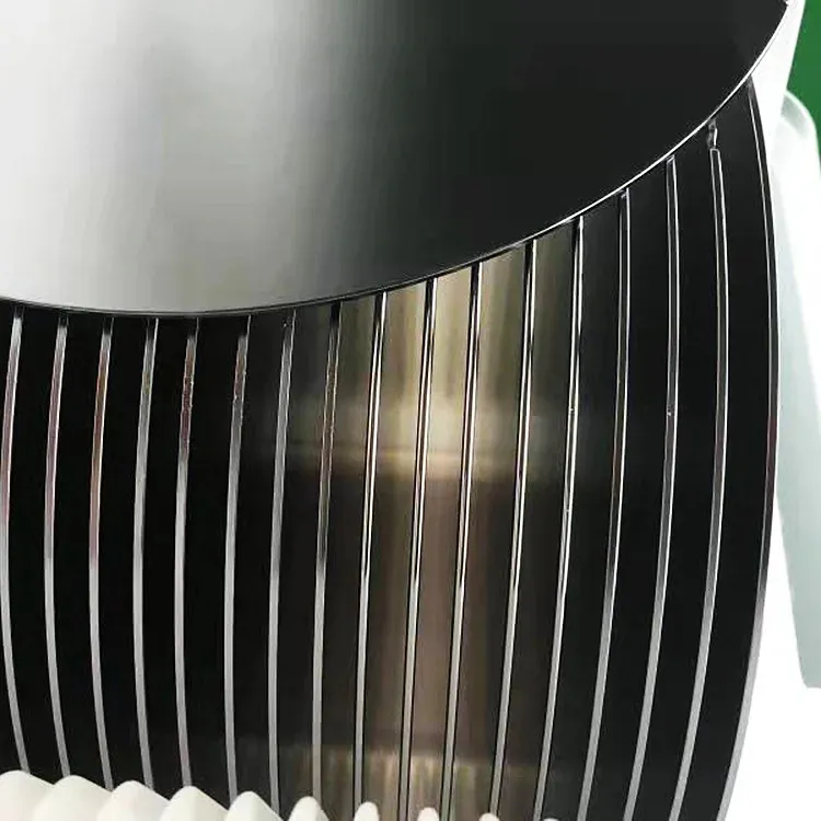
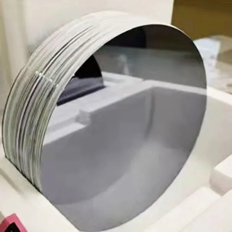
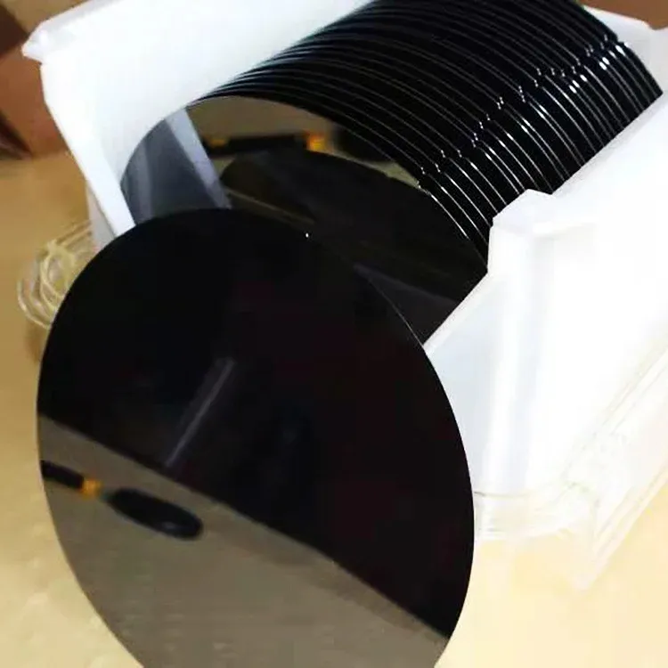
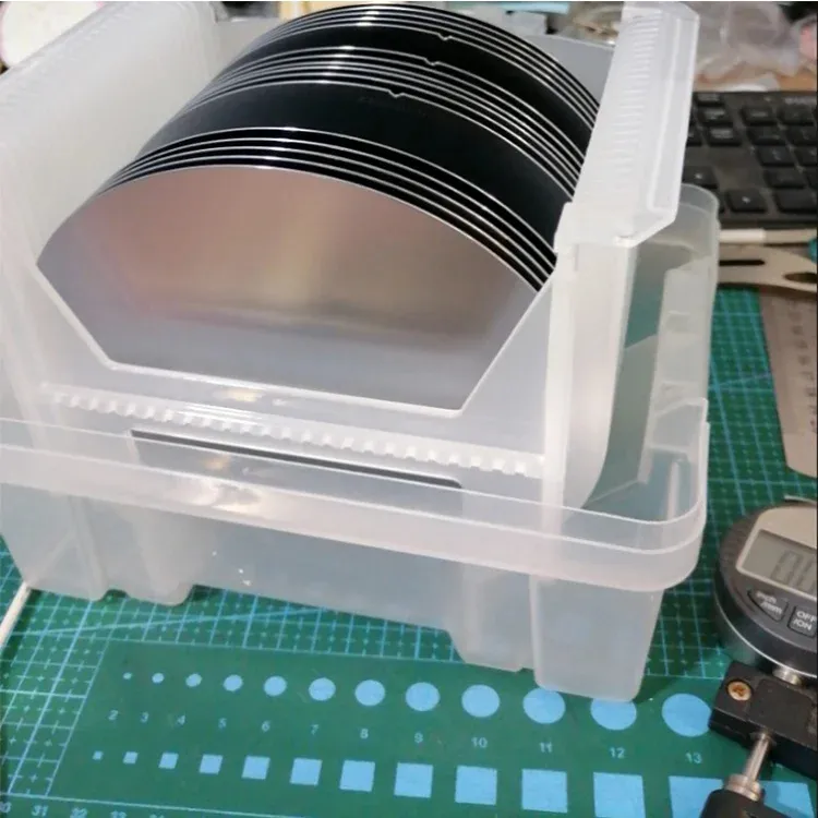
- "2-12" SEMI-standard dummy wafers fit seamlessly with existing lithography, etching, and deposition equipment in academic labs.
- Polished surfaces with Ra < 0.5nm and customizable oxide/metal coatings (50nm-5μm) replicate production-grade substrate conditions.
- ISO Class 5 cleanroom-certified dummy wafers with <0.3 particles/ft³ (≥0.5μm) for GMP-compliant research.
- Reclaim service restores used wafers to 95% of original specs, cutting long-term material costs by 35% for repeatable processes.
Table of Contents
1. Introduction to Dummy Wafers
In the intricate realm of semiconductor manufacturing and research, Dummy Wafers play a pivotal yet often understated role. A Dummy Wafer is a non – functional wafer specifically designed to mimic the physical and chemical properties of actual semiconductor wafers used in device fabrication, such as those made of silicon, gallium arsenide, or silicon carbide. However, unlike their functional counterparts, Dummy Wafers do not carry the integrated circuits that are the end – goal of semiconductor production.
These wafers are an essential tool across a wide range of applications, from academic research labs exploring the frontiers of semiconductor technology to industrial production facilities aiming to optimize their manufacturing processes. Their significance lies in their ability to provide a cost – effective and low – risk platform for various operations that are critical to the semiconductor workflow.
2. Types of Dummy Wafers
2.1 Silicon Dummy Wafers
Silicon is the most prevalent material in the semiconductor industry, and silicon Dummy Wafers are accordingly the most commonly used type. They come in a variety of sizes, ranging from as small as 2 inches to as large as 12 inches in diameter, conforming to the industry – standard SEMI specifications. This wide size range ensures compatibility with different semiconductor equipment, whether it’s a small – scale research tool in a university lab or a large – scale production machine in a manufacturing plant.
Silicon Dummy Wafers are available in different thicknesses and surface finishes. For applications that require a smooth surface for processes like thin – film deposition or lithography, polished silicon wafers with surface roughness values as low as Ra < 1nm can be provided. In other cases, where the focus is more on mechanical handling or bulk material testing, wafers with rougher surface finishes may be used. Their versatility makes them suitable for a broad spectrum of semiconductor processes, from basic equipment calibration to advanced process development.
2.2 Silicon – on – Insulator (SOI) Dummy Wafers
SOI Dummy Wafers are designed for specialized semiconductor fabrication processes that demand high – performance features. These wafers consist of a thin layer of silicon on top of an insulating layer, typically silicon dioxide. The insulating layer provides improved electrical isolation between different components on the wafer, which is crucial for reducing power consumption and improving the speed of semiconductor devices.
While SOI Dummy Wafers are less commonly used compared to silicon Dummy Wafers due to their higher cost, they are indispensable in research and development settings for high – end semiconductor applications. For example, in the development of advanced microprocessors or high – frequency communication devices, SOI Dummy Wafers are used to test and optimize processes such as deep – sub – micron lithography and ultra – low – power circuit design.
2.3 Imitation Dummy Wafers
Imitation Dummy Wafers, often made from materials other than traditional semiconductor materials, are primarily used for non – semiconductor applications. They are a cost – effective alternative for educational institutions and training facilities where the goal is to teach students or new employees the basic handling and processing techniques of semiconductor wafers without the need for expensive real – deal wafers.
These imitation wafers are available in various sizes, although they may not always adhere strictly to the industry – standard dimensions used in actual semiconductor manufacturing. They are designed to replicate the physical appearance and some basic handling characteristics of real wafers, allowing trainees to gain practical experience in a low – risk and budget – friendly environment.
2.4 Photonic Dummy Wafers
Photonic Dummy Wafers are tailored for the production and development of photonic devices, which are integral to applications such as optical communication, sensing, and computing. These wafers are typically fabricated from materials like silicon, lithium niobate, or indium phosphide, which have excellent optical properties.
In the manufacturing of photonic integrated circuits (PICs), Photonic Dummy Wafers are used to test and ensure the compatibility of equipment during the development phase. They help in optimizing processes such as the deposition of optical waveguides and the fabrication of optical modulators, which are key components in PICs. By using Photonic Dummy Wafers, researchers and manufacturers can reduce the cost and time associated with developing new photonic device designs.
3. Key Functions of Dummy Wafers
3.1 Testing and Calibration of Equipment
Semiconductor manufacturing equipment, such as lithography machines, etchers, and deposition systems, requires precise calibration to ensure accurate and consistent processing of wafers. Dummy Wafers are used as sacrificial substrates for this purpose. Before running expensive production wafers through the equipment, Dummy Wafers are processed first.
Engineers can then analyze the results on the Dummy Wafers, such as the quality of a deposited film, the accuracy of an etched pattern, or the uniformity of an ion – implanted layer. Based on these analyses, they can adjust the equipment parameters, such as temperature, pressure, gas flow rates, or laser exposure times, to achieve the desired performance. This not only saves the cost of potentially ruining valuable production wafers but also ensures that the equipment is in optimal condition for high – volume production.
3.2 Process Development and Optimization
The semiconductor industry is constantly evolving, with new manufacturing processes being developed to improve device performance, reduce costs, and increase production yields. Dummy Wafers are invaluable in this process development phase.
Engineers can experiment with different process parameters, such as chemical concentrations in wet etching processes, plasma power in dry etching, or deposition rates in chemical vapor deposition (CVD), using Dummy Wafers. By analyzing the resulting wafer characteristics, such as surface roughness, film thickness uniformity, or pattern fidelity, they can identify the optimal process conditions. This approach allows for rapid iteration and optimization of processes without the high cost associated with using production – grade wafers. Once the optimal process parameters are determined, they can be transferred to production, leading to more efficient and cost – effective manufacturing.
3.3 Equipment Maintenance and Contamination Control
Regular maintenance of semiconductor manufacturing equipment is essential to ensure its long – term reliability and performance. Dummy Wafers are used during maintenance procedures to perform tests and checks. For example, after equipment cleaning or component replacement, Dummy Wafers are processed to verify that the equipment has been restored to its proper working condition.
Moreover, semiconductor manufacturing is a highly sensitive process, and even minute amounts of contamination can lead to device failures. Dummy Wafers are used to monitor and control contamination in the manufacturing environment. They can be run through the equipment at regular intervals, and then analyzed for the presence of particles, chemicals, or other contaminants. If contamination is detected, appropriate cleaning or maintenance procedures can be implemented to prevent it from affecting production wafers.
3.4 Yield Improvement and Risk Mitigation
In semiconductor manufacturing, yield improvement is a continuous challenge. Defects in the manufacturing process can lead to a significant number of non – functional devices, increasing costs and reducing profitability. Dummy Wafers help in yield improvement by allowing manufacturers to identify and address potential issues before they affect production wafers.
For instance, in high – risk processes such as ion implantation, where incorrect process parameters can cause irreparable damage to wafers, Dummy Wafers are used first to test the process. If problems are detected, such as non – uniform ion implantation or excessive wafer heating, the process can be adjusted before exposing production wafers to the same conditions. This proactive approach helps in reducing the defect rate and improving the overall yield of the manufacturing process.
4. Applications in Academic and Research Settings
4.1 Nanotechnology Research
In nanotechnology research, where the goal is to manipulate and control materials at the nanoscale level, Dummy Wafers are used to develop and test new fabrication techniques. For example, in the creation of nanowires or quantum dots on a wafer surface, researchers use Dummy Wafers to optimize the deposition and growth processes.
They can vary parameters such as the temperature, pressure, and precursor gas composition during chemical vapor deposition or molecular beam epitaxy on Dummy Wafers. By analyzing the resulting nanostructures using techniques like scanning electron microscopy and atomic force microscopy, they can determine the optimal conditions for fabricating high – quality nanostructures on production wafers. This research is crucial for the development of next – generation semiconductor devices with enhanced performance, such as more efficient solar cells or faster transistors.
4.2 Photonics and Optoelectronics Research
In the field of photonics and optoelectronics, which focuses on the interaction of light with semiconductor materials, Dummy Wafers are used for a variety of purposes. In the development of optical waveguides, which are used to guide light in integrated optical circuits, Dummy Wafers are used to test different waveguide designs and fabrication processes.
Researchers can deposit and pattern various materials on Dummy Wafers to create waveguide structures and then measure their optical properties, such as light propagation loss and mode confinement. This information is used to optimize the design and fabrication of optical waveguides for applications in optical communication, optical sensing, and optical computing. Similarly, in the development of optoelectronic devices like light – emitting diodes (LEDs) and photodetectors, Dummy Wafers are used to optimize the epitaxial growth processes and device fabrication steps.
4.3 MEMS (Micro – Electro – Mechanical Systems) Fabrication
MEMS devices, which integrate mechanical and electrical components on a microscopic scale, require precise fabrication processes. Dummy Wafers are extensively used in MEMS fabrication for process development and optimization.
For example, in the fabrication of micro – channels for fluidic applications or micro – cantilevers for sensing applications, Dummy Wafers are used to test etching and deposition processes. By adjusting parameters such as the etchant concentration, etching time, and deposition temperature on Dummy Wafers, engineers can achieve the desired MEMS structure dimensions and surface qualities. This is crucial for the reliable and cost – effective production of MEMS devices, which are used in a wide range of applications, from automotive airbag sensors to smartphone accelerometers.
5. Our Product Offerings and Advantages
5.1 Wide Range of Sizes and Materials
We offer Dummy Wafers in a comprehensive range of sizes, including 2 – inch, 4 – inch, 6 – inch, 8 – inch, and 12 – inch diameters, all of which adhere to the strict SEMI standards. This ensures seamless compatibility with your existing semiconductor equipment, whether you are working in a small – scale research laboratory or a large – scale production facility.
In terms of materials, we provide Dummy Wafers made from high – purity silicon, as well as other semiconductor materials such as gallium arsenide, silicon carbide, and sapphire. Each material has its unique properties, making them suitable for different applications. For example, gallium arsenide is ideal for high – frequency and optoelectronic applications, while silicon carbide is preferred for high – power and high – temperature applications. Our diverse material options allow you to choose the Dummy Wafer that best suits your specific research or production needs.
5.2 Customization Options
Understanding that each research project or manufacturing process may have unique requirements, we offer extensive customization options for our Dummy Wafers. We can customize the thickness of the wafers, with options ranging from as thin as 100μm to as thick as 1mm, depending on your application.
In addition, we provide a variety of surface finishes, including polished surfaces for applications that require smooth interfaces for thin – film deposition or lithography, and textured surfaces for applications where enhanced adhesion or specific surface properties are desired. We can also apply different coatings, such as oxide, nitride, or metal layers, to the wafer surface to meet your specific process requirements. Whether you need a specific edge profile, such as chamfered or beveled edges, or custom markings for identification purposes, our team of experts can work with you to provide a tailored solution.
5.3 High – Quality and Consistency
Quality is at the core of our Dummy Wafer production. Each wafer undergoes a rigorous manufacturing process to ensure high – quality and consistent performance. Our state – of – the – art manufacturing facilities are equipped with advanced equipment and staffed by experienced engineers and technicians who adhere to strict quality control procedures.
Before leaving our facility, each Dummy Wafer is thoroughly tested for parameters such as thickness uniformity, surface roughness, and flatness. We also provide detailed certificates of analysis (COAs) for each batch of wafers, which include information on the wafer’s physical and chemical properties, as well as the results of our quality control tests. This ensures that you receive Dummy Wafers that meet the highest industry standards and perform consistently in your applications.
5.4 Competitive Pricing and Fast Delivery
We understand the importance of cost – effectiveness and timely delivery in your research and production operations. That’s why we offer Dummy Wafers at competitive prices without compromising on quality. Our efficient supply chain management and economies of scale allow us to provide you with high – quality wafers at affordable rates.
In addition, we strive to offer fast delivery times. For standard – sized Dummy Wafers that are in stock, we can typically process and ship your order within 3 – 5 business days. For customized wafers, our lead times are as short as 1 – 2 weeks, depending on the complexity of the customization. We also offer rush order services for those urgent projects, with expedited processing available to ensure you receive your wafers in as little as 2 – 3 days. Our commitment to competitive pricing and fast delivery makes us the ideal partner for all your Dummy Wafer needs.
Faqs:
1. 1. What is a Dummy Wafer and why do we need it?
A Dummy Wafer is a non-functional semiconductor wafer used for process development, equipment calibration, or training. It mimics the physical properties (size, thickness, material) of actual wafers without integrated circuits, allowing researchers to test processes like deposition, etching, or lithography without wasting expensive functional wafers.
2. What materials are Dummy Wafers available in?
We offer Dummy Wafers in common semiconductor materials, including:
- Silicon (Si)
- Gallium Arsenide (GaAs)
- Silicon Carbide (SiC)
- Sapphire (Al₂O₃)
- Glass substrates
Custom materials can be arranged based on specific research needs.
3. What standard sizes do Dummy Wafers come in?
Our standard sizes include:
- 2-inch (50.8mm)
- 4-inch (100mm)
- 6-inch (150mm)
- 8-inch (200mm)
- 12-inch (300mm)
All sizes meet SEMI standards for compatibility with common lab equipment.
4. Can Dummy Wafers be customized for specific experiments?
Yes. We provide customization for:
- Thickness (ranging from 100μm to 1mm)
- Surface finishes (polished, rough, or textured)
- Coatings (oxide, nitride, or metal layers)
- Edge profiles (chamfered or beveled)
Contact us with your requirements for a tailored solution.
5. How do Dummy Wafers help with process optimization?
Dummy Wafers allow researchers to:
- Test process parameters (temperature, pressure, gas flow) without risking functional wafers
- Calibrate equipment like sputtering systems or ion implanters
- Train staff on handling and processing techniques
This reduces costs and accelerates research by minimizing material waste.
6. What is the typical lead time for Dummy Wafer orders?
- Standard sizes (in stock): 3-5 business days
- Customized wafers: 1-2 weeks (depending on complexity)
- Rush orders: Expedited processing available for urgent needs (2-3 days)
Contact our sales team for specific timelines.
7. How are Dummy Wafers packaged for international shipping?
- Individual wafers: Sealed in anti-static poly bags with desiccant
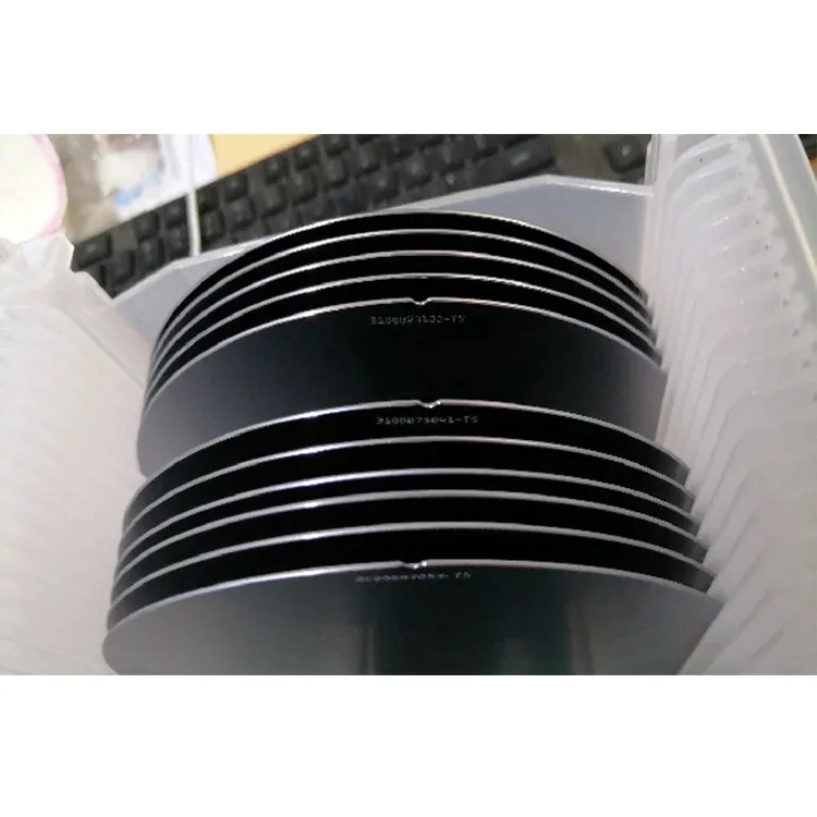
- Multiple wafers: Stacked in polystyrene cassettes or wafer boats
- Outer packaging: Sturdy cardboard boxes with shock-absorbing foam
- Shipping: Tracked services via DHL, FedEx, or UPS with export documentation (e.g., commercial invoices, packing lists).
8. Can Dummy Wafers be reused for multiple experiments?
Yes, depending on the process:
- Dry processes (e.g., lithography, deposition): Reusable after cleaning
- Wet processes (e.g., etching, chemical treatments): May require surface re-polishing
We offer wafer reclaim services to restore used dummy wafers for repeated use, reducing long-term costs.
9. What is the price range for Dummy Wafers?
Prices vary by size and material, Contact us for details.
10. Are Dummy Wafers compatible with automated wafer handling systems?
Yes, all standard-size wafers are designed for:
- Robotic wafer loaders
- Cassette-based processing equipment
- Vacuum chuck systems
Custom edge profiles can be adapted for specific handling mechanisms.
11. Can you assist with technical specifications for our research project?
Yes, our technical team can help:
- Recommend materials based on process requirements
- Suggest surface finishes for optimal adhesion
- Provide guidelines for wafer cleaning and handling
Contact us with your project details for personalized support.
REQUEST A QUOTE
Our professional team will reply to you within one business day. Please feel free to contact us!
