
Wafer Jar
The Ideal Choice Designed for Semiconductor Wafers. Each wafer jar is rigorously tested to ensure exceptional protection during transportation and storage, preventing static and physical damage. Whether in research laboratories or production lines, these wafer jars provide safe and reliable solutions. Choose our wafer jars to ensure that every wafer is ready to meet the technological challenges of the future in optimal condition!
- Supports small-batch customization and exclusive services for laboratories
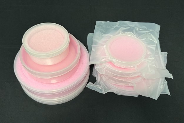
- Dust-free vacuum packaging, ready for immediate use
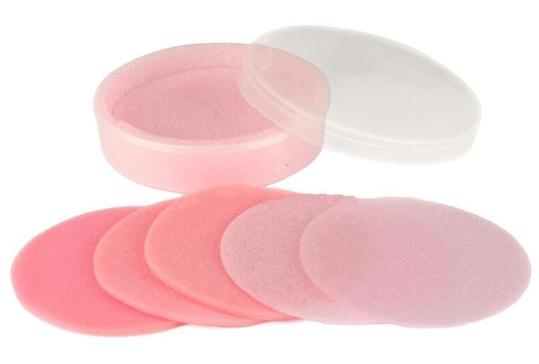
Wafer Jar Structure Details:
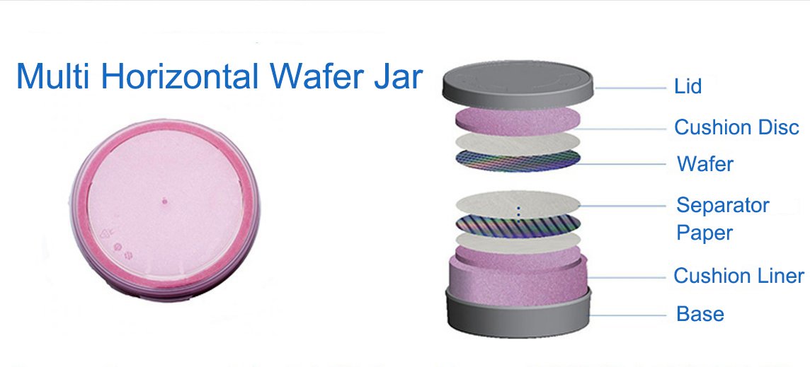
- The upper and lower covers are designed to facilitate the operator’sopening and ensure the secure during transportation.
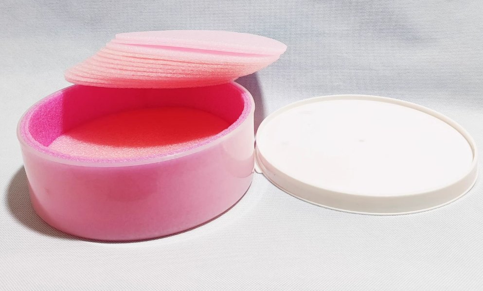
- Foam liner/isolator packagingis used to improve the shock-proofability and provide effective protection for wafer transportation.
- The design can effectively reduce the overall weight whilebeautifying the appearance
- The font is concave below the surface, effectively avoiding the risk ofbreaking HDPE bags during transportation.
Efficient Protection Technology
Our wafer jars use advanced anti-static materials and design for exceptional wafer protection during transport and storage. Key features include:
- Anti-Static Performance
Treated surfaces inhibit static electricity buildup, preventing damage and ensuring accurate experimental results. - Cushioning Protection
Internal cushioning materials absorb shocks, reducing physical damage during transport. - Strong Sealing
Precision seals keep out dust and contaminants, maintaining a clean environment during storage.
- Anti-Static Performance
Flexible Customization Options
Our wafer jars offer flexible small-batch customization to meet the specific needs of laboratories:
Tailored Sizes
We provide various sizes to ensure a perfect fit with laboratory equipment.Material Selection
Customers can choose materials based on their specific applications, such as varying anti-static properties.Small-Batch Production
Flexible purchasing options allow labs to order as needed without maintaining large inventories.- Custom Printing
Personalized printing, including logos and barcodes, helps with laboratory management.
Dust-Free Vacuum Packaging
Our wafer jars utilize dust-free vacuum packaging technology to ensure that each jar can be used immediately after opening. Key features include:
Strict Cleaning Process
Before packaging, the wafer jars undergo a rigorous cleaning and disinfection process to ensure that both the surface and interior are free of contaminants, providing the highest level of cleanliness.Vacuum Sealing
The vacuum sealing technology prevents air and external contaminants from entering the jar, ensuring a pure internal environment and reducing the risk of wafer contamination during storage and transport.
Convenient Storage Design
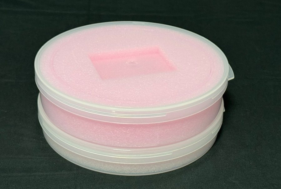
- Modular Structure
The wafer jars are designed to be modular, allowing for easy stacking and combination in the laboratory, maximizing space utilization and reducing footprint, thereby improving overall lab layout efficiency. - Labeling System
Each wafer jar includes a designated area for labeling, making it easy to record and identify different types and statuses of wafers, simplifying laboratory management and improving management efficiency.
- Modular Structure
Wafer Jar Packaging
- Temperature Resistance
Materials offer excellent stability under varying conditions to meet diverse lab needs. - Transparent Window
Each wafer jar is equipped with a transparent window, facilitating quick identification of the internal wafer condition, allowing for rapid assessment of wafer integrity, thus reducing search time and enhancing work efficiency. - Quick Delivery
Optimized processes ensure fast delivery of customized orders to meet urgent requirements.
- Temperature Resistance
Wafer Jar FAQs:
1. How to clean a wafer jar correctly?
When cleaning, use a dust – free cloth dipped in high – purity reagents (such as ultrapure water, isopropyl alcohol) to wipe, and avoid using ordinary cleaning agents. If there are stubborn stains remaining inside the jar, it can be immersed in a diluted hydrofluoric acid solution (only for corrosion – resistant materials). Finally, rinse thoroughly with ultrapure water and dry it to ensure there are no particle residues.
2. What is the sealing principle of a wafer jar?
It usually adopts O – ring seals, flange seals, or vacuum sealing structures. The O – ring seal achieves physical sealing through elastic extrusion; the vacuum seal creates a negative pressure by evacuating the air inside the jar, isolating external contaminants, and is often used for storing wafers sensitive to water vapor and oxygen.
3. Can a wafer jar be reused?
Yes, it can. But after each use, it needs to be thoroughly cleaned, tested for airtightness, and checked for any physical damage (such as scratches, cracks). If it is used for different types of wafers (such as common silicon wafers and compound semiconductors), additional cross – contamination testing is required.
4. How to choose the appropriate size of a wafer jar?
Choose according to the wafer size (such as 8 – inch, 12 – inch), storage quantity, and process requirements. Ensure that there is enough space for the wafer inside the jar to avoid contact with the jar wall; also consider the compatibility with equipment, such as whether it can fit into storage cabinets or glove boxes.
5. What are the requirements for the storage environment of a wafer jar?
The ideal environment is a cleanroom (Class 100 or higher cleanliness), with the temperature controlled at 20 – 25°C and the relative humidity < 40%. Avoid direct sunlight or proximity to heat sources to prevent material aging or wafer thermal deformation; also keep it away from organic solvents, corrosive gases, and other pollution sources.
6. What safety precautions should be taken when using a wafer jar in the laboratory?
When using it in the laboratory, wear dust – free gloves to avoid contaminating the wafers with hand grease; handle it gently to prevent the wafers from cracking due to collisions. If storing toxic or radioactive wafers, special labels should be attached, and laboratory safety procedures should be followed.
7. Can a wafer jar be used to store non - semiconductor wafer materials?
Theoretically, it can be used, but it is necessary to ensure that the materials are compatible with the jar material and there is no risk of contamination. For example, it can be used to store optical lenses, ultra – thin slices for scientific research, etc., but avoid using it interchangeably with semiconductor wafers to prevent cross – contamination.
8. How to detect the airtightness of a wafer jar?
Common methods include helium mass spectrometer leak detection, pressure decay testing, or humidity monitoring. The helium mass spectrometer leak detector determines the sealing performance by detecting the helium leakage; the pressure decay test observes the pressure change inside the jar; humidity monitoring judges whether there is water vapor penetration from the outside by recording the internal humidity over a long period.
9. What is the service life of a wafer jar?
The service life depends on the frequency of use, cleaning and maintenance conditions, and environmental conditions. Under normal circumstances, a quartz – made wafer jar can be used for 3 – 5 years, and a PFA – made one can be used for 2 – 3 years. If there is seal failure, material aging, or physical damage, it should be replaced immediately.
10. Can a wafer jar be placed in a high - temperature furnace to process wafers?
It depends on the material. A quartz – made wafer jar can withstand high temperatures, up to over 1000°C; while a PFA – made one has a lower temperature resistance, usually below 260°C and cannot be used for high – temperature processing. Before use, be sure to confirm the material’s heat resistance limit and the wafer process requirements.
11. How to disinfect a wafer jar in the laboratory?
In the laboratory, disinfection can be carried out by UV irradiation (suitable for transparent materials), plasma treatment, or fumigation with low – concentration hydrogen peroxide vapor. Avoid directly wiping with organic solvents such as alcohol to prevent residue from contaminating the wafers. If chemical disinfectants are used, rinse thoroughly and dry.
12. Is a wafer jar anti - static?
Some wafer jars add anti – static materials (such as carbon – doped PFA) or use anti – static coatings, which are suitable for storing wafers sensitive to static electricity. When purchasing, confirm whether the product has anti – static markings or parameter descriptions.
13. Can wafer jars be stacked for storage?
It is not recommended to stack them casually, especially when storing valuable wafers. Stacking may cause uneven stress on the lower jars, affecting airtightness or damaging the wafers. If space needs to be saved, use a special stacking rack and ensure uniform load – bearing and strong stability.
14. How to handle discarded wafers in a wafer jar?
Discarded wafers need to be sorted for disposal: ordinary silicon wafers can be recycled as general solid waste; wafers containing heavy metals, radioactive substances, or chemical pollutants need to be handled by professional institutions in accordance with laboratory hazardous waste management procedures, and random disposal is strictly prohibited.
15. Can a wafer jar be used in a vacuum environment?
Some wafer jars are designed to be vacuum – compatible and can be used for vacuum storage or transfer of wafers. Before use, confirm the product specifications and work with vacuum pumps, vacuum valves, and other equipment to achieve vacuum sealing, preventing wafers from being damaged by air pressure differences in a vacuum environment.
REQUEST A QUOTE
Our professional team will reply to you within one business day. Please feel free to contact us!
