
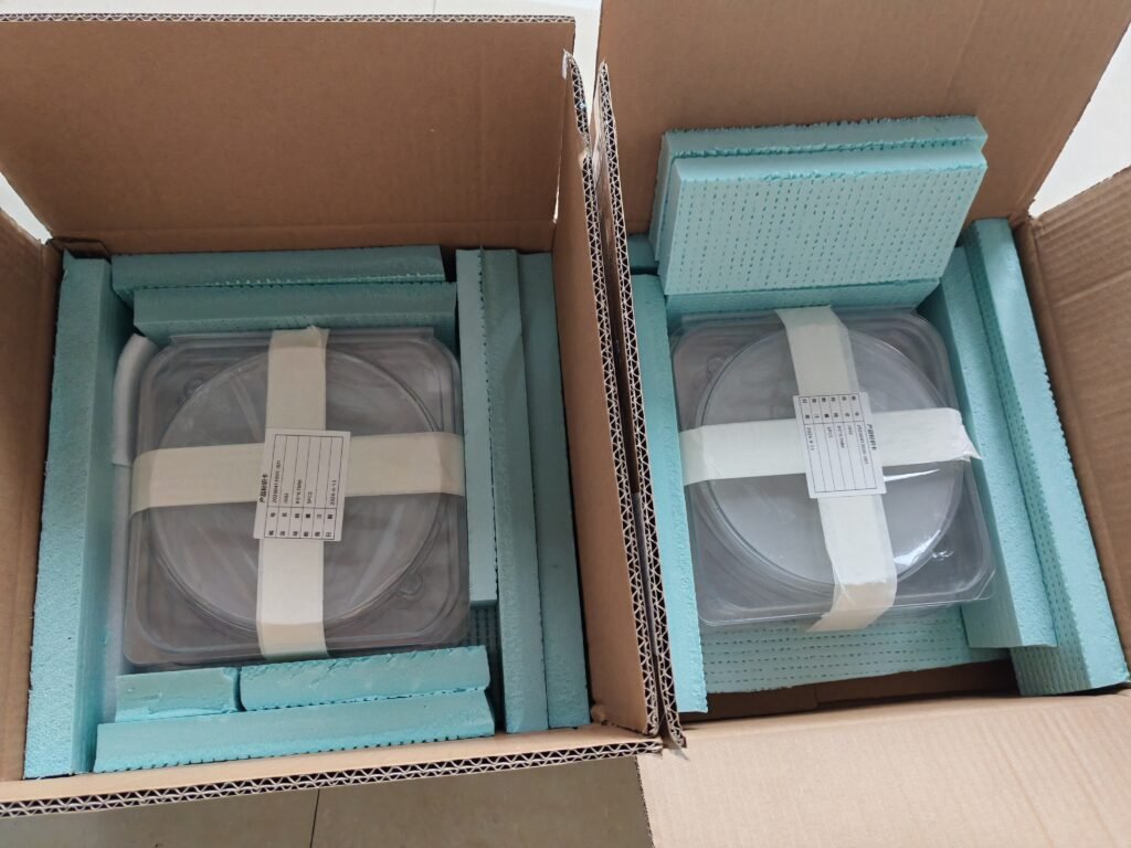
We are pleased to announce that a batch of 8-inch JGS2 grade fused silica wafers has been successfully shipped to Munster Technological University, Ireland, to support their cutting‑edge scientific research and engineering experiments.
What is JGS2 Fused Silica?
Fused silica (fused quartz) wafers are high‑performance optical substrates widely used in precision optics, semiconductors, MEMS, photonics, and laboratory R&D.
JGS2 is a standard optical grade with key advantages:
- Excellent optical transmission from ultraviolet to near‑infrared
- High thermal stability and low thermal expansion coefficient
- Good chemical resistance and mechanical stability
- Suitable for coating, lithography, microfabrication, and optical testing
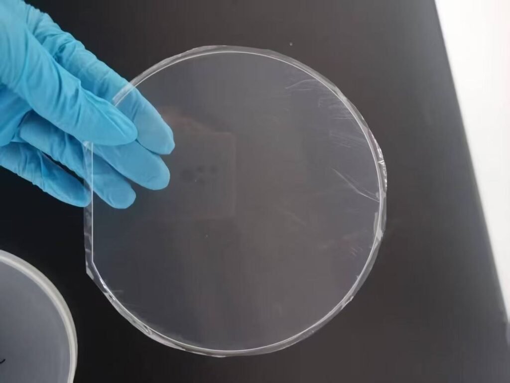
These characteristics make JGS2 fused silica wafers ideal for academic research, prototype development, and high‑precision component manufacturing.
We are proud to support global universities and research institutions with reliable, high‑purity substrate solutions. We look forward to more innovative collaborations in semiconductor, photonic, and MEMS R&D worldwide.
Do you need a custom JGS2 wafer specification for your research or project? We can provide a tailored quote right away.
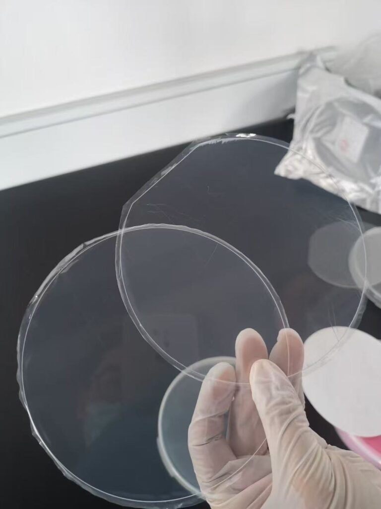
We support full customization of fused silica wafers in various sizes and shapes. Available diameters include 1-inch, 2-inch, 4-inch, 6-inch, 8-inch, 12-inch, and even larger formats. Thickness can also be customized to your exact requirements. Our MOQ starts from just 1 piece, fully matching small-batch testing and R&D needs in laboratories.
