
Mention “silicon,” and most people immediately envision chips and computers. It’s true—today’s digital world is built upon silicon-based integrated circuits, and silicon’s status as the bedrock of semiconductors is indisputable. However, if you think silicon’s capabilities end there, you are underselling the element that makes up over a quarter of the Earth’s crust. When light meets high-quality silicon, a brilliant optoelectronic symphony unfolds within the infrared spectrum. This is the world of Optical Grade Silicon.
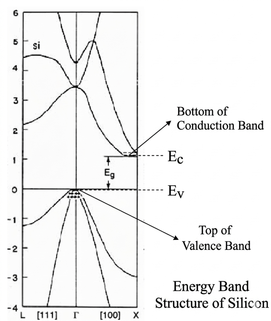
So, why silicon? With a bandgap of approximately 1.12 eV, silicon is virtually “invisible” to infrared light with wavelengths exceeding 1.1 μm. The photon energy is insufficient to excite valence electrons into the conduction band, meaning it escapes the grip of intrinsic absorption. In other words, in the near-infrared and mid-infrared bands, pure silicon is almost perfectly transparent. Leveraging this unique “optical window,” optical grade silicon excels in fields like infrared imaging, thermal detection, laser transmission, and fiber optic communications, serving as a vital bridge between the optical and electronic worlds.
Today, let’s explore this “Invisible Giant”—Optical Grade Silicon Materials.
I. Fundamentals of Physics
When discussing optical grade silicon, the conversation inevitably centers on transmittance. The ability of a seemingly opaque silicon wafer to transmit infrared light is determined by two critical factors.
1. Making Silicon “Transparent”: Understanding the Constraints of Transmittance
Reflection Loss: The First Hurdle
Silicon possesses an exceptionally high
refractive index, approximately 3.4 (which remains nearly constant across the infrared spectrum). When infrared light travels from air () to a silicon surface, a significant portion is reflected according to Fresnel’s equations. Even without considering any internal absorption, the theoretical maximum transmittance of a double-side polished silicon wafer is only about 52%—nearly half the light is lost at the surfaces. This is why most infrared optical components must be treated with Anti-Reflection (AR) coatings to effectively “unlock” silicon’s transparency potential.
Free Carrier Absorption: The Core Driver of Resistivity Requirements
Free Carrier Absorption (FCA) refers to the phenomenon where free electrons (dominant in N-type silicon) and holes (dominant in P-type silicon) within the crystal lattice absorb infrared photons, much like a sponge soaking up water. The higher the doping concentration, the greater the number of free carriers, and the more pronounced the absorption becomes. In other words, to achieve “optical clarity” in silicon, the doping concentration must be minimized—which translates to
increasing the resistivity.
Both theory and practice have established clear quantitative boundaries:
• For N-type silicon: Resistivity must exceed .
• For P-type silicon: Requirements are more stringent, needing to exceed to surpass the 45% transmittance threshold.
To pursue even higher transmittance—approaching the theoretical limit of 52%—materials with higher resistivity and superior purity are required. Furthermore, distinguishing between N-type and P-type is of significant engineering importance because electrons and holes have different infrared absorption characteristics. This is the underlying physical reason why P-type silicon requires higher resistivity than N-type silicon to achieve comparable optical performance.
II. Manufacturing Processes for Optical Grade Silicon
Building upon the physical principles discussed above, let’s explore the “origins” of optical grade silicon—the crystal growth processes. Currently, there are two primary technological routes: the Czochralski (CZ) Method and the Float-Zone (FZ) Method. The materials produced by these two methods each have their own unique strengths and characteristics.
1. The Czochralski (CZ) Method: The King of Yield
The Czochralski method, also known as the CZ method, is the most mainstream and widely used technique for producing monocrystalline silicon, accounting for approximately 80% of all silicon crystal production.
The principle is straightforward: polycrystalline silicon raw material is melted in a quartz crucible. A tiny seed crystal is then dipped into the melt and slowly pulled upward while rotating. The melt undergoes directional crystallization at the end of the seed, eventually growing into a massive, cylindrical monocrystalline silicon ingot.
The Advantages of CZ Silicon:
Large Diameter: It can produce large-diameter ingots, meeting the demands of large-scale industrial production.
Cost-Effectiveness: The production costs are relatively low compared to other methods.
The “Inherent Weakness”:
The primary drawback of the CZ method is the unavoidable introduction of oxygen impurities from the quartz crucible. Oxygen impurities cause characteristic absorption bands at specific wavelengths (most notably around 9μm) and can affect the overall optical uniformity of the material. Consequently, while CZ silicon is reliable enough for infrared applications in the 3-5 μm band, more precise optical systems operating at longer wavelengths may require alternative materials.
2. The Float-Zone (FZ) Method: The Choice for High Purity
If the Czochralski method is the “King of Yield,” then the Float-Zone (FZ) method is undoubtedly the “King of Purity.” The principle behind the FZ method is quite ingenious: a polycrystalline silicon rod is fixed vertically, and a small section of it is heated to a molten state using a high-frequency induction heater. This molten zone is then moved slowly along the length of the rod. By exploiting the difference in segregation coefficients of impurities between the liquid and solid phases, the impurities are effectively “swept” to one end, much like “washing” the material.
Because the silicon melt never comes into contact with a crucible during the entire process, it avoids contamination from oxygen, carbon, and other impurities found in quartz containers. As a result, the FZ method can produce monocrystalline silicon with extremely low oxygen content and ultra-high purity, with resistivity easily exceeding 1,000 Ω·cm or even higher. Of course, the trade-off is that the crystal diameter is limited (usually not exceeding 150mm), and the production cost is significantly higher than that of the CZ method.
If we compare the CZ method to a “high-volume chef” providing plenty for everyone, the FZ method is more like a “meticulous craftsman” refining a masterpiece. Both have their own vital roles to play, and neither is inherently superior to the other.
III. The Stages of Application for Optical Grade Silicon
Having understood its physical properties and manufacturing processes, let’s look at where this “invisible expert” truly shines.
Infrared Windows and Lenses: The Classic Applications
Silicon lenses and window plates are widely used in optical systems operating within the 2-7 μm band. Whether it is the lens of a thermal imager, the window of an infrared thermometer, or the coupling lens for an infrared LED, optical grade silicon is indispensable. With a density of only 2.33 g/cm3—roughly half that of Germanium—silicon is especially favored in aerospace and other weight-sensitive applications.
Smart Driving and Security Monitoring: Emerging Frontiers
In recent years, silicon lenses have become a cornerstone of autonomous driving and surveillance. Infrared automotive cameras equipped with silicon optics help self-driving systems “see” the road clearly under harsh conditions such as night or thick fog. Meanwhile, security thermal imaging equipment utilizes infrared silicon components for 24/7 continuous target monitoring and recognition. These technologies are becoming increasingly ubiquitous, finding their way into consumer electronics like smartphones and smart door locks.
Healthcare and Medical Diagnostics
The medical field also relies heavily on optical grade silicon. From non-invasive infrared temperature monitoring to optical components in sophisticated diagnostic equipment, silicon supports the core functions of numerous medical instruments thanks to its excellent thermal conductivity and chemical stability.
Silicon Photonics: The Cutting Edge
Silicon photonics represents the most advanced frontier for this material. Driven by the explosive demand for Artificial Intelligence (AI) computing power, silicon photonics technology is moving from the laboratory to large-scale industrialization. Projections indicate that the global silicon photonics market will grow from approximately $2.65 billion in 2025 to about $9.65 billion by 2030, with a compound annual growth rate (CAGR) of nearly 30%. By integrating electronic and optical functions onto a single platform, silicon photonic chips are expected to break through the bandwidth and power consumption limits of traditional electronic chips, becoming the core technology for next-generation data communications.
IV. Clarifying Common Misconceptions
To ensure a precise understanding of optical grade silicon, it is important to address these three common industry myths.
Misconception 1: Optical Grade Silicon and Electronic Grade Silicon are Interchangeable.
The Fact: This is not the case. Electronic Grade Silicon (EGS) is optimized for electrical performance—carrier mobility, precise dopant control, and low defect density. In contrast, the core requirements for Optical Grade Silicon are infrared transmittance and optical homogeneity.
While they may originate from the same crystal growth technology, their resistivity specifications and quality control standards are entirely different. Silicon used in microchips typically has a resistivity of only 1-20Ω·cm, which is often “insufficiently transparent” for high-end infrared optics. Conversely, the “luxuriously high” resistivity of optical grade silicon is unnecessary for standard integrated circuits. When selecting materials, precision is key.
Misconception 2: High-Resistivity Silicon is Transparent Across All Wavelengths.
The Fact: This statement requires a physical caveat. While high resistivity effectively suppresses Free Carrier Absorption, the crystal lattice itself imposes a “ceiling.” As wavelengths exceed approximately 8μm, light enters the phonon absorption region of the silicon crystal. At this point, regardless of how high the resistivity is, the silicon will gradually lose its transparency. This is why the effective upper limit for the transmission band of optical grade silicon is roughly 8μm.
Misconception 3: Float-Zone (FZ) Silicon is Always Superior to Czochralski (CZ) Silicon.
The Fact: This depends entirely on the specific application. While the high-purity, oxygen-free nature of FZ silicon is a significant advantage, it is not always necessary. For applications operating in the 3-5 μm band, the oxygen absorption band of CZ silicon (located at 9 μm) presents no obstacle at all—because the operating wavelength is nowhere near the absorption peak.
Choosing FZ silicon without a specific technical requirement often results in significantly higher costs without any tangible performance gain. The wise choice is to apply the right material to the right challenge.
