ABS Wafer Frame

ABS Wafer Frame
Introduction to ABS Wafer Frame
ABS Wafer Frames are pivotal components in the semiconductor field, serving as essential carriers for holding and securing wafers. They play an indispensable role in both academic research and industrial production. Composed primarily of acrylonitrile – butadiene – styrene (ABS) copolymer, these frames are widely adopted due to the material’s outstanding comprehensive properties.
Key Features of ABS Wafer Frames
1. Mechanical Properties
Impact Resistance
The unique molecular structure of ABS endows wafer frames with exceptional shock absorption capabilities. During the handling and processing of semiconductor wafers, vibrations and collisions are inevitable. The two – phase structure of ABS, featuring rubbery polybutadiene domains dispersed in a rigid acrylonitrile – styrene matrix, allows it to dissipate impact energy effectively.
With an impact strength of 15 – 25 kJ/m² (as per ASTM D256), ABS frames can withstand drops from 0.5 meters or accidental mechanical collisions without fracturing. This effectively safeguards wafers from cracks and edge chipping, significantly improving semiconductor device yield rates and typically maintaining them above 95%.
Dimensional Stability
ABS exhibits excellent dimensional stability across diverse environments and complex manufacturing processes. It has a glass transition temperature (Tg) of approximately 105°C and a low coefficient of thermal expansion (8×10⁻⁵/°C).
Even under thermal cycling between 25°C – 60°C, which is common in lithography and etching processes, ABS frames maintain precise geometries. Thanks to the material’s low crystallinity (5 – 10%), shrinkage variations are minimized. For example, during the chemical mechanical polishing (CMP) of 8 – inch wafers, ABS frames ensure positioning accuracy within ±2 μm.
Chemical Resistance
The nitrile (-CN) and aromatic ring groups in ABS provide robust chemical resistance. In aggressive environments like 10% hydrofluoric acid (HF) used in wet etching, ABS forms a passivation layer. After 24 – hour immersion, its mass loss is limited to <0.3%.
Moreover, ABS resists swelling or embrittlement from common solvents such as isopropyl alcohol (IPA) and acetone. This enables repeated ultrasonic or spray cleaning without performance degradation.
2. Size Specifications
To meet diverse semiconductor process requirements, ABS Wafer Frames are available in standard sizes:
- 4 – inch
- 6 – inch
- 8 – inch
- 12 – inch
These dimensions adhere to industry – wide standards, ensuring compatibility with semiconductor wafer processing, storage, and transportation. Whether for small – scale academic research or large – scale IC manufacturing, appropriate frame sizes can be readily selected.
3. Customization Capabilities
Recognizing the unique demands of research and specialized production, we offer comprehensive customization services for ABS Wafer Frames. Our customization options include:
- Dimension Adjustment: Tailoring frame sizes to fit non – standard wafers precisely.
- Marking Solutions: Incorporating specialized markings for enhanced wafer identification and tracking.
- Material Optimization: Modifying material properties to withstand specific temperature, humidity, or chemical conditions, enabling adaptation to cutting – edge semiconductor applications.
4. Application Scenarios
ABS Wafer Frames are integral throughout the semiconductor manufacturing process:
- Wafer Fabrication: They provide stable platforms for critical processes such as crystal growth, photolithography, and etching, ensuring process precision and consistency.
- Chip Packaging: ABS frames facilitate accurate alignment between wafers and packaging materials, enhancing overall packaging quality.
- Storage & Transportation: These frames protect wafers from environmental degradation during storage and physical damage during transit, supporting the efficient and stable development of the semiconductor industry.
Faqs
1. What standard sizes does your ABS wafer frame product line cover?
2. Is customization available for ABS wafer frames used in specialized experiments?
3. What material constitutes your ABS wafer frames?
4. How do ABS wafer frames perform in high – temperature scenarios?
5. Are ABS wafer frames compatible with different types of semiconductor wafers?
6. What is the load – bearing capacity of ABS wafer frames?
7. How should I clean and maintain ABS wafer frames?
8. What is the shelf life of ABS wafer frames?
10. How are ABS wafer frames packaged for safe transportation?
11. What is the lead time for delivering ABS wafer frames?
13. Can ABS wafer frames be used in cleanroom environments?
14. Do ABS wafer frames have anti – static properties?
15. How do ABS wafer frames compare in cost to other types of wafer frames?
16. Can I order samples of ABS wafer frames before placing a large order?
related products
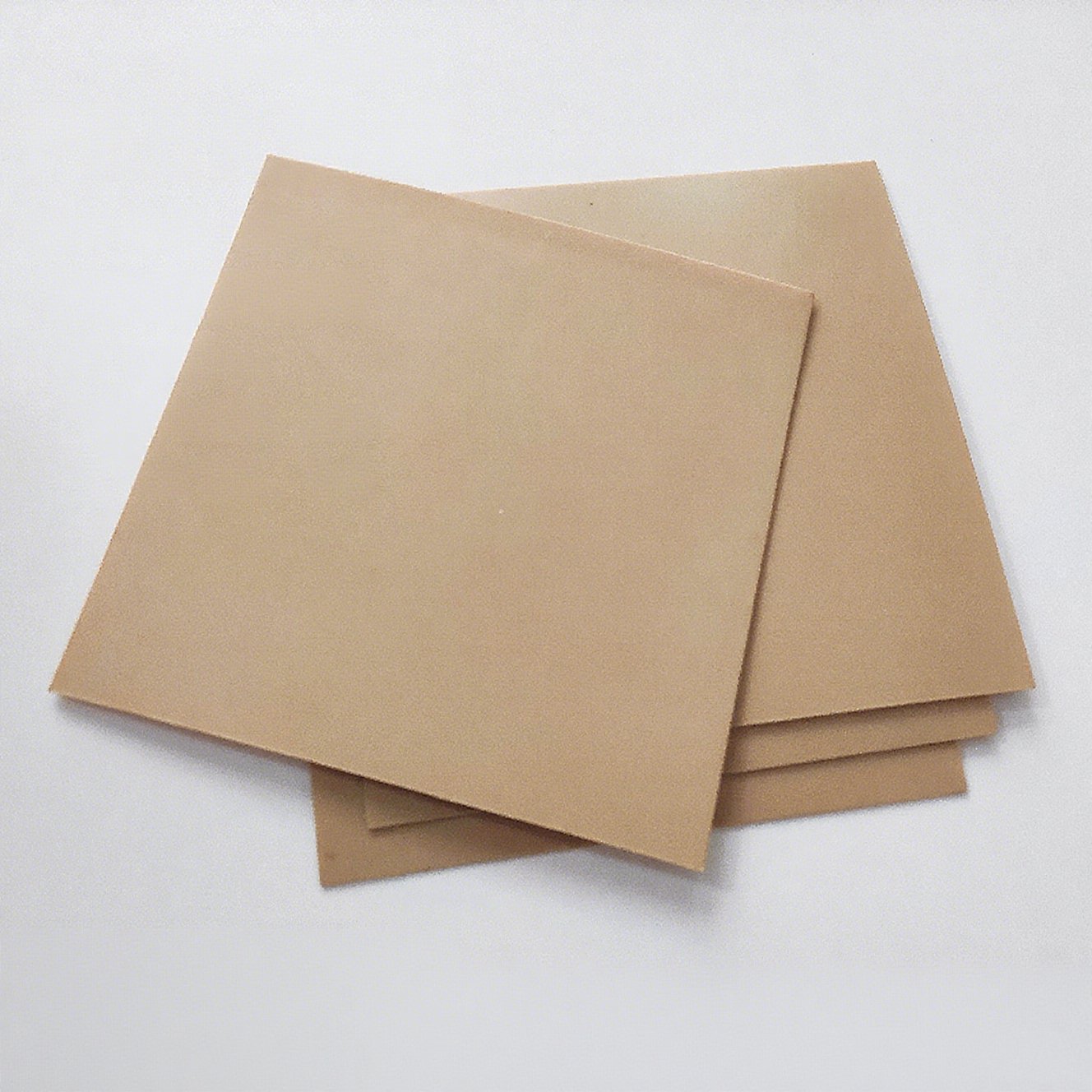
Peek Plastic Sheet
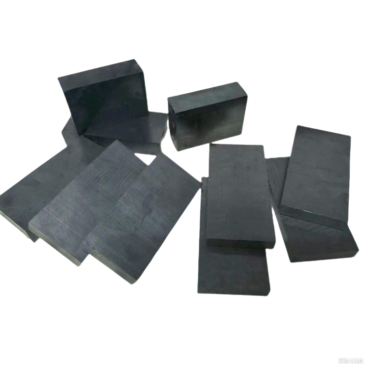
Black Peek Sheet
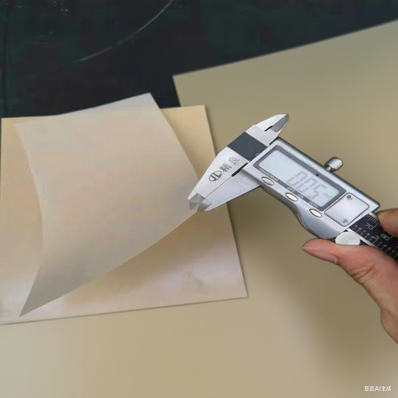
Peek Sheet 2mm

Peek Sheet 1mm
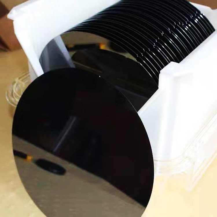
silicon dummy wafer
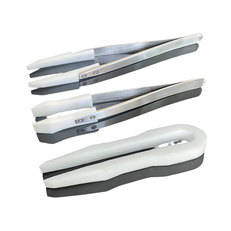
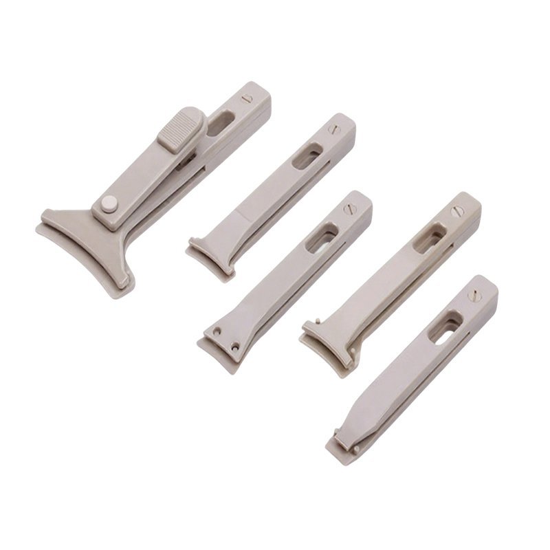
Teflon Wafer Tweezers
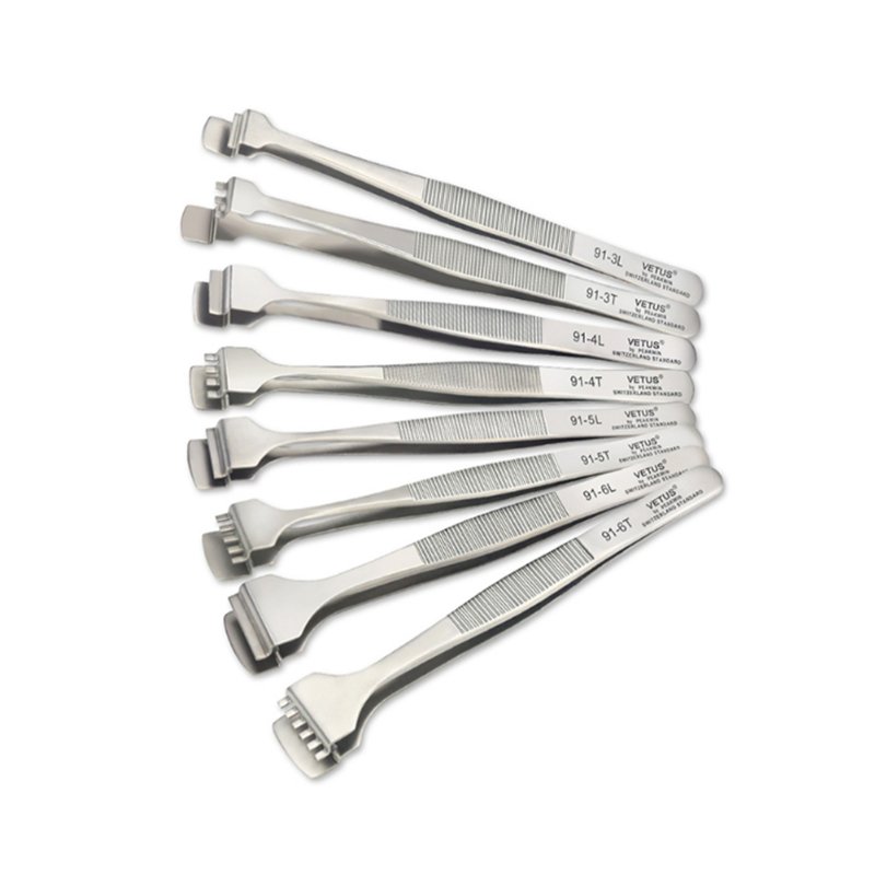
Wafer Forceps